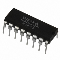
IXBD4411PI IXYS, IXBD4411PI Datasheet - Page 5

IXBD4411PI
Manufacturer Part Number
IXBD4411PI
Description
IC HIGH SIDE DRIVER 16DIP
Manufacturer
IXYS
Series
ISOSMART™r
Type
Isolated Half Bridge Driver Chip Setr
Datasheet
1.IXBD4410PI.pdf
(11 pages)
Specifications of IXBD4411PI
Configuration
High-Side
Input Type
Non-Inverting
Delay Time
110ns
Current - Peak
2A
Number Of Configurations
1
Number Of Outputs
1
High Side Voltage - Max (bootstrap)
1200V
Voltage - Supply
10 V ~ 20 V
Operating Temperature
-40°C ~ 85°C
Mounting Type
Through Hole
Package / Case
16-DIP (0.300", 7.62mm)
Product
Half-Bridge Drivers
Rise Time
100 ns
Fall Time
150 ns
Supply Voltage (min)
10 V
Maximum Power Dissipation
600 mW
Maximum Operating Temperature
+ 85 C
Mounting Style
Through Hole
Bridge Type
Half Bridge
Minimum Operating Temperature
- 40 C
Number Of Drivers
1
Output Current
2 A
Lead Free Status / RoHS Status
Lead free / RoHS Compliant
© 2004 IXYS All rights reserved
the IXBD4411 is strictly for status only.
Any gate-drive shutdown because of a
high-side fault is done
high-side IXBD4411. The IXBD4411
gate-drive will turn-off the power device
whenever an overcurrent or under
voltage condition arises. The overcurrent
sensing is active only while the gate
driver output is "high" (on). The
overcurrent fault condition is latched and
is reset on the next INH gate input
positive transition. The FLT (pin 8) of the
IXBD4411 is not used and should be
grounded.
The low-side IXBD4410 driver provides
an output pin 8 (FLT) to indicate a high-
side (IXBD4411) or a low-side
(IXBD4410) fault. This output pin is an
"open-drain" output. The IXBD4410 low-
side driver fault indications are similar to
the IXBD4411 high-side driver indications
as outlined above. A "graphic" logic
diagram of the chipset's FLT function is
presented in Fig.4. Note that this diagram
presents the logic of this function at the
"low-side" IXBD4410 driver and is not the
actual circuit. It describes the combined
logic of the "fault logic" and "hi-side fault
sense" blocks in both the IXBD4410 and
IXBD4411 as shown in Fig. 2 and 3.
The most efficient method of providing
power for the high-side driver is by
bootstrapping. This method is illustrated
in the functional drawing on page 4 and
in the application example (Fig. 6 and 9)
by diode D1 and capacitor C1. Using this
method, the power is drawn through a
high-voltage diode onto a reservoir
capacitor whenever the floating high-side
ground returns to near the real ground of
the low-side driver. When the high-side
gate is turned on and the floating ground
moves towards a higher potential, the
bootstrapping diode back-biases, and the
high-side driver draws its power solely
from the reservoir capacitor. Power may
also be provided via any isolated power
supply (usually an extra secondary on
the system housekeeping supply
switching transformer).
Both the IXBD4410 and IXBD4411
contain on-board negative charge pumps
to provide negative gate drive, which
ensures turn-off of the high- or low-side
power device in the presence of currents
induced by power device Miller capaci-
tance or from inductive ground transients.
These charge pumps provide -5 V
relative to the local driver ground when
locally within the
V
currents of 25 mA. The charge pump
requires two external capacitors, C7 and
C11 in Fig. 6. The charge pump
frequency is nominally 600 kHz. The
charge pump clock is turned off
whenever the difference between the V
and V
exceeding the breakdown rating of the
IC.
Both the IXBD4410 and IXBD4411
drivers possess two local grounds each,
a common logic ground, and "Kelvin"
ground. The Kelvin ground and logic
grounds are first connected directly to
each other, and then to the Kelvin-source
of the power device for accurate over-
current measurement in the presence of
inductive transients on the power device
source terminal.
Power MOSFET or IGBT overcurrent
sensing utilizes an on-chip comparator
with a typical 300 mV threshold. In a
typical application, the current mirror pin
of the Power MOSFET or IGBT is con-
nected to a grounded, low-value resistor,
and to the overcurrent comparator input
on the high- or low-side driver. The
comparator will respond typically within
150 ns to an overcurrent condition to
shutdown the driver output. The power
switches could be protected also by
desa-turation detection (see Fig. 6, 7 and
9).
To assure maximum protection for the
phase-leg power devices, the chipset
incorporates the following Power
MOSFET and IGBT protection circuits:
DD
Power device overcurrent or desa-
turation protection. The IXBD4410/
4411will turn off the driven device
within 150 ns of sensing an output
overcurrent or desaturation condition.
Gate-drive lockout circuitry to prevent
cross conduction (simultaneous
conduction of the low- and high-side
phase-leg power devices), either
under normal operating conditions or
when a fault occurs.
During power-up, the chipset's gate-
drive outputs will be low (off), until the
voltage reaches the under-voltage trip
point.
Under-voltage gate-drive lockout on
the low- and/or high- side driver when-
ever the respective positive power
supply falls below 9.5 V typically.
Under-voltage gate-drive lockout on
the low- and high- side driver
whenever the respective negative
power supply rises above -3 V
typically.
is at +15 V, and at rated average
EE
supplies exceed 20 V, to prevent
DD
IXBD4410
IXBD4411
5


