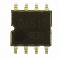
BD6517F-E2 Rohm Semiconductor, BD6517F-E2 Datasheet - Page 5

BD6517F-E2
Manufacturer Part Number
BD6517F-E2
Description
IC SWITCH HIGH SIDE 2CH SOP-8
Manufacturer
Rohm Semiconductor
Type
High Sider
Specifications of BD6517F-E2
Input Type
Non-Inverting
Number Of Outputs
2
On-state Resistance
110 mOhm
Current - Output / Channel
500mA
Current - Peak Output
1.65A
Voltage - Supply
3 V ~ 5.5 V
Operating Temperature
-25°C ~ 85°C
Mounting Type
Surface Mount
Package / Case
8-SOP
Power Load Switch Type
High Side
Input Voltage
5.5V
On Resistance Rds(on)
0.11ohm
On / Enable Input Polarity
Active Low
Power Dissipation Pd
560mW
No. Of Outputs
2
Current Limit
1.65A
Supply Voltage (min)
3 V
Supply Voltage (max)
5.5 V
Supply Current (typ)
100 uA
Operating Temperature Range
- 25 C to + 85 C
Mounting Style
SMD/SMT
On State Resistance
0.11ohm
Rohs Compliant
Yes
Lead Free Status / RoHS Status
Lead free / RoHS Compliant
Lead Free Status / RoHS Status
Lead free / RoHS Compliant, Lead free / RoHS Compliant
Other names
BD6517F-E2TR
Available stocks
Company
Part Number
Manufacturer
Quantity
Price
Part Number:
BD6517F-E2
Manufacturer:
ROHM/罗姆
Quantity:
20 000
Measurement circuit
© 2009 ROHM Co., Ltd. All rights reserved.
BD6512F,BD6513F,BD6516F,BD6517F,BD2042AFJ,BD2052AFJ
www.rohm.com
◎BD6512F/ BD6513F/ BD6516F/ BD6517F
◎BD2042AFJ/ BD2052AFJ
V
V
V
V
V
V
CTRL
CTRL
CTRL
CTRL
EN
EN
ON resistance, Over current detection
ON resistance, Over current detection
V
DD
10k
V
V
1µF
EN
EN
A
GND
IN
EN1
EN2
V
CTRLA
FLAGA
FLAGB
CTRLB
DD
V
10k
Operating current
Operating current
DD
1µF
CTRLA
FLAGA
FLAGB
CTRLB
GND
IN
EN1
EN2
OUT1
OUT2
OUTB
/OC1
/OC2
OUTA
GND
VDD
10k
OUTB
OUTA
OUT1
OUT2
GND
VDD
/OC1
/OC2
A
10k
V
V
1µF
1µF
DD
DD
I
OUT
I
V
OUT
DD
Fig.1 Measurement circuit
I
I
OUT
OUT
C
C
L
L
5/20
V
V
CTRL
CTRL
V
V
V
V
CTRL
CTRL
EN
EN
EN, /EN input voltage, Output rise, fall time
V
V
I
CTRL input voltage, Output rise, fall time
FLAG
V
EN
EN
DD
V
1µF
DD
CTRLA
FLAGA
FLAGB
CTRLB
GND
IN
EN1
EN2
1µF
/OC output LOW voltage
FLAG output resistance
GND
IN
EN1
EN2
I
FLAG
CTRLA
FLAGA
FLAGB
CTRLB
OUTB
OUTA
GND
VDD
OUT1
OUT2
/OC1
/OC2
OUT1
OUT2
/OC1
/OC2
I
OUT
OUTB
R
OUTA
GND
V
VDD
L
1µF
DD
2009.05 - Rev.A
Technical Note
C
L
I
OUT
R
R
R
L
L
L
V
1µF
C
DD
L
C
C
L
L


