VNV35N07 STMicroelectronics, VNV35N07 Datasheet - Page 3
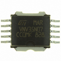
VNV35N07
Manufacturer Part Number
VNV35N07
Description
MOSFET N-CH 70V 35A POWERSO-10
Manufacturer
STMicroelectronics
Series
OMNIFET™r
Type
Low Sider
Datasheet
1.VNV35N07.pdf
(13 pages)
Specifications of VNV35N07
Input Type
Non-Inverting
Number Of Outputs
1
On-state Resistance
28 mOhm
Current - Peak Output
35A
Mounting Type
Surface Mount
Package / Case
PowerSO-10 Exposed Bottom Pad
Switch Type
Low Side
Power Switch Family
VNV35N07
Input Voltage
18V
Power Switch On Resistance
35mOhm
Output Current
25A
Mounting
Surface Mount
Supply Current
250uA
Package Type
PowerSO
Pin Count
10
Power Dissipation
125W
Lead Free Status / RoHS Status
Contains lead / RoHS non-compliant
Voltage - Supply
-
Operating Temperature
-
Current - Output / Channel
-
Lead Free Status / Rohs Status
Not Compliant
Other names
497-3319-5
Available stocks
Company
Part Number
Manufacturer
Quantity
Price
Company:

Part Number:
VNV35N07
Manufacturer:
TOSHIBA
Quantity:
2 679


ELECTRICAL CHARACTERISTICS (continued)
SWITCHING ( )
SOURCE DRAIN DIODE
PROTECTION
( ) Pulsed: Pulse duration = 300 s, duty cycle 1.5 %
( ) Parameters guaranteed by design/characterization
Symb ol
Symb ol
I
Symb ol
(di/dt)
t
T
V
T
E
Q
RRM
dl im
I
t
t
t
j sh
t
t
r r
j rs
gf
SD
as
d(on)
d(of f)
d(on)
d(of f)
r r
I
Q
(
(
lim
t
t
t
t
(
(
(
(
r
f
r
f
(
(
i
( )
on
)
)
)
)
)
)
)
)
Turn-on Delay Time
Rise Time
Turn-off Delay Time
Fall T ime
Turn-on Delay Time
Rise Time
Turn-off Delay Time
Fall T ime
Turn-on Current Slope
Total Input Charge
Forward O n Voltage
Reverse Recovery
Time
Reverse Recovery
Charge
Reverse Recovery
Current
Drain Current Limit
Step Response
Current Limit
Overtemperature
Shutdown
Overtemperature Reset
Fault Sink Current
Single Pulse
Avalanche Energy
Parameter
Parameter
Parameter
V
V
(see figure 3)
V
V
(see figure 3)
V
V
V
I
I
V
(see test circuit, figure 5)
V
V
V
V
V
V
starting T
V
SD
SD
DD
gen
DD
gen
DD
i n
DD
DD
i n
i n
i n
i n
i n
i n
i n
= 10 V
= 18 A
= 18 A
= 10 V
= 5 V
= 10 V
= 5 V
= 10 V
= 5 V
= 10 V R
= 28 V
= 28 V
= 28 V
= 12 V
= 30 V
= 10 V
= 10 V
j
Test Cond ition s
Test Cond ition s
Test Cond ition s
= 25
V
V
V
V
V
I
gen
di/dt = 100 A/ s
DS
DS
D
in
DS
DS
T
R
I
D
j
o
R
R
= 18 A
I
I
gen
= 0
C
d
d
= 25
= 13 V
= 13 V
= 1 K
= 18 A
= 13 V
= 13 V
gen
gen
= 18 A
= 18 A
= 10
= 10
= 1000
V
o
C
DD
V
= 20 V
L = 10 mH
i n
VNP35N07FI-VNB35N07-VNV35N07
= 10 V
Min.
Min.
Min.
150
135
2.5
25
25
Typ .
Typ .
Typ .
100
350
650
200
500
100
250
2.7
4.3
10
60
35
35
35
70
50
20
1
8
Max.
1000
Max.
Max.
200
600
350
800
140
4.2
6.5
1.6
16
45
45
60
A/ s
Un it
Un it
Un it
mA
mA
nC
o
o
ns
ns
ns
ns
ns
ns
V
A
A
A
J
C
C
C
s
s
s
s
s
3/13
Related parts for VNV35N07
Image
Part Number
Description
Manufacturer
Datasheet
Request
R

Part Number:
Description:
STMicroelectronics [RIPPLE-CARRY BINARY COUNTER/DIVIDERS]
Manufacturer:
STMicroelectronics
Datasheet:
Part Number:
Description:
STMicroelectronics [LIQUID-CRYSTAL DISPLAY DRIVERS]
Manufacturer:
STMicroelectronics
Datasheet:

Part Number:
Description:
BOARD EVAL FOR MEMS SENSORS
Manufacturer:
STMicroelectronics
Datasheet:
Part Number:
Description:
NPN TRANSISTOR POWER MODULE
Manufacturer:
STMicroelectronics
Datasheet:
Part Number:
Description:
TURBOSWITCH ULTRA-FAST HIGH VOLTAGE DIODE
Manufacturer:
STMicroelectronics
Datasheet:
Part Number:
Description:
Manufacturer:
STMicroelectronics
Datasheet:
Part Number:
Description:
DIODE / SCR MODULE
Manufacturer:
STMicroelectronics
Datasheet:
Part Number:
Description:
DIODE / SCR MODULE
Manufacturer:
STMicroelectronics
Datasheet:
Part Number:
Description:
Search -----> STE16N100
Manufacturer:
STMicroelectronics
Datasheet:
Part Number:
Description:
Search ---> STE53NA50
Manufacturer:
STMicroelectronics
Datasheet:
Part Number:
Description:
NPN Transistor Power Module
Manufacturer:
STMicroelectronics
Datasheet:
Part Number:
Description:
DIODE / SCR MODULE
Manufacturer:
STMicroelectronics
Datasheet: