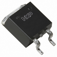
BUK108-50DL,118 NXP Semiconductors, BUK108-50DL,118 Datasheet

BUK108-50DL,118
Specifications of BUK108-50DL,118
BUK108-50DL /T3
BUK108-50DL /T3
Related parts for BUK108-50DL,118
BUK108-50DL,118 Summary of contents
Page 1
... D T Continuous junction temperature j R Drain-source on-state resistance DS(ON) I Input supply current ISL FUNCTIONAL BLOCK DIAGRAM INPUT LOGIC AND PROTECTION Fig.1. Elements of the TOPFET. PIN CONFIGURATION Product specification BUK108-50DL MAX. UNIT 150 ˚C 125 650 A IS DRAIN O/V CLAMP POWER ...
Page 2
... CONDITIONS ˚ inductive load ˚ 250 Hz DD CONDITIONS Human body model 250 pF 1.5 k the over temperature trip operates to protect the switch. j(TO) is less than V maximum. DS DDP(P) 2 Product specification BUK108-50DL MIN. MAX. UNIT - 13 8 -55 150 ˚C - 150 ˚C - 250 ˚C MIN. MAX. ...
Page 3
... 300 0. 125 ˚ 7 300 0.01 CONDITIONS ˚ from I 0 CONDITIONS 7 300 0.01 3 Product specification BUK108-50DL MIN. TYP. MAX. UNIT - 2.5 3.1 K K/W MIN. TYP. MAX. UNIT 0 100 125 m MIN. TYP. MAX. UNIT - 0 0 150 - - ˚C MIN. TYP. MAX. UNIT Rev 1.000 ...
Page 4
... T 25 ˚ CONDITIONS 300 not applicable CONDITIONS Measured from upper edge of tab to centre of die Measured from source lead soldering point to source bond pad 4 Product specification BUK108-50DL MIN. TYP. MAX. 1.0 1.5 2 100 200 350 160 270 ˚C 2.0 2.6 3 150 ˚C 1 ...
Page 5
... Fig.7. Typical on-state resistance Product specification BUK108-50DL BUK108-50DL D = 0.5 0.2 0.1 0.05 0. 1E-05 1E-03 1E- f(t); parameter j-mb p BUK108-50DL VIS / VDS / f(V ); parameter BUK108-50DL VIS / 4.5 3 ˚ f(I ); parameter DS(ON 1E+01 6 5.5 5 4 ˚ Rev 1.000 ...
Page 6
... Fig.12. Typical clamping characteristics, 25 ˚ ˚ 100 120 140 - IS(TO) 6 Product specification BUK108-50DL Time / ms Tj(TO) Energy / J - 100 140 180 Tmb / load = BUK108-50DL typ. 60 VDS / V = f(V ); conditions VIS(TO max. typ. min. -40 - 100 120 140 Fig.13. Input threshold voltage. = f(T ); conditions mA BUK108-50DL 220 Rev 1.000 ...
Page 7
... Fig.18. Normalised limiting clamping energy ˚ DSM = 250 s p VDS VIS 0 D.U.T. 0V 0R1 Fig.19. Clamping energy test circuit Product specification BUK108-50DL BUK108-50DL VDS VIS 100 200 300 time / ˚ 100 120 Tmb / f(T ); conditions V(CL)DSS VDD + L VDS - D TOPFET D.U.T. ...
Page 8
... Fig.20. Typical off-state leakage current f(T ); Conditions DSS j DS June 1996 Iiso & Iisl normalised 1.5 typ. 1 0.5 100 120 140 -60 Fig.21. Normalised input currents (normal & latched ISO 8 Product specification BUK108-50DL - 100 140 25˚C & 25˚ ISO ISL ISL j IS 180 Rev 1.000 ...
Page 9
... Plastic meets UL94 V0 at 1/8". June 1996 10.3 max 11 max 15.4 0.85 max (x2) Fig.22. SOT404 : centre pin connected to mounting base. 11.5 9.0 2.0 3.8 5.08 Fig.23. SOT404 : minimum pad sizes for surface mounting . 9 Product specification BUK108-50DL 4.5 max 1.4 max 2.5 0.5 17.5 Rev 1.000 ...
Page 10
... Philips customers using or selling these products for use in such applications their own risk and agree to fully indemnify Philips for any damages resulting from such improper use or sale. June 1996 10 Product specification BUK108-50DL Rev 1.000 ...


