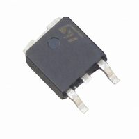
VND3NV04 STMicroelectronics, VND3NV04 Datasheet - Page 8

VND3NV04
Manufacturer Part Number
VND3NV04
Description
MOSFET POWER OMNIFET II DPAK
Manufacturer
STMicroelectronics
Series
OMNIFET II™r
Type
Low Sider
Datasheet
1.VNN3NV0413TR.pdf
(26 pages)
Specifications of VND3NV04
Input Type
Non-Inverting
Number Of Outputs
1
On-state Resistance
120 mOhm
Current - Peak Output
5A
Mounting Type
Surface Mount
Package / Case
DPak, TO-252 (2 leads+tab), SC-63
Switch Type
Low Side
Power Switch Family
VND3NV04
Power Switch On Resistance
120mOhm
Output Current
3.5A
Mounting
Surface Mount
Supply Current
100uA
Package Type
DPAK
Pin Count
2 +Tab
Power Dissipation
35W
Lead Free Status / RoHS Status
Lead free / RoHS Compliant
Voltage - Supply
-
Operating Temperature
-
Current - Output / Channel
-
Lead Free Status / Rohs Status
Not Compliant
Available stocks
Company
Part Number
Manufacturer
Quantity
Price
Company:
Part Number:
VND3NV04-1
Manufacturer:
ST
Quantity:
12 500
Company:
Part Number:
VND3NV04-1-E
Manufacturer:
ST
Quantity:
26 000
Company:
Part Number:
VND3NV04-1-E
Manufacturer:
STMicroelectronics
Quantity:
1 816
Company:
Part Number:
VND3NV04-E
Manufacturer:
ST
Quantity:
12 000
Company:
Part Number:
VND3NV0413TR
Manufacturer:
ST
Quantity:
26 000
Electrical specifications
Table 4.
1. Pulsed: Pulse duration = 300 µs, duty cycle 1.5 %
8/26
Source drain diode (T
Protections (-40 °C < T
Symbol
(dI/dt)
V
t
t
t
t
I
t
d(on)
d(off)
d(on)
d(off)
RRM
T
SD
T
E
Q
I
dlim
Q
I
t
lim
t
t
t
t
jsh
gf
rr
jrs
as
r
f
r
f
rr
i
(1)
on
Turn-on delay time
Rise time
Turn-off delay time
Fall time
Turn-on delay time
Rise time
Turn-off delay time
Fall time
Turn-on current slope
Total input charge
Forward on voltage
Reverse recovery time
Reverse recovery charge
Reverse recovery current
Drain current limit
Step response current
limit
Over temperature
shutdown
Over temperature reset
Fault sink current
Single pulse avalanche
energy
Electrical characteristics (continued)
Parameter
j
=25 °C, unless otherwise specified)
j
< 150 °C, unless otherwise specified)
V
V
(see figure
V
V
(see figure
V
V
V
I
I
I
V
(see test circuit, figure
V
V
V
starting T
V
(see figures
gen
SD
SD
DD
gen
DD
gen
DD
gen
DD
DD
IN
IN
IN
IN
=1.5 A; V
=1.5 A; dI/dt=12 A/µs
=5 V; V
=5 V; V
=5 V; V
=5 V R
=2.13 mA (see figure
=15 V; I
=15 V; I
=15 V; I
=12 V; I
=30 V; L=200 µH
=5 V; R
=5 V; R
=5 V; R
Doc ID 7382 Rev 3
j
=25µ°C; V
gen
DS
DS
DS
Figure
Figure
D
D
D
D
gen
gen
gen
Figure 6.
IN
Test conditions
=1.5 A
=1.5 A
=1.5 A
=1.5 A; V
=13 V
=13 V
=13 V; T
=R
=0 V
=R
=2.2 KΩ
=R
IN MIN
VNN3NV04, VNS3NV04, VND3NV04, VND3NV04-1
IN MIN
IN MIN
4.)
4.)
DD
j
=220 Ω; L=24 mH
&
=T
IN
Figure
=24 V
=220 Ω
=220 Ω
Figure
=5 V
jsh
Figure
5.)
8.)
7.)
Min
150
135
100
3.5
10
0.45
Typ
250
450
250
107
175
2.5
3.3
2.0
4.7
8.5
0.8
0.7
90
37
10
15
5
1350
Max
1.35
10.0
300
750
750
200
7.5
6.0
20
7
A/µs
Unit
mA
mJ
nC
µC
ns
ns
ns
µs
µs
µs
µs
ns
µs
°C
°C
ns
V
A
A


