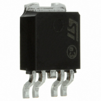
VN751PT STMicroelectronics, VN751PT Datasheet - Page 11

VN751PT
Manufacturer Part Number
VN751PT
Description
IC DRIVER HIGHSIDE 2.5A PPAK-5
Manufacturer
STMicroelectronics
Type
High Sider
Datasheet
1.VN751PT13TR.pdf
(17 pages)
Specifications of VN751PT
Input Type
Non-Inverting
Number Of Outputs
1
On-state Resistance
60 mOhm
Current - Output / Channel
2.5A
Current - Peak Output
6A
Voltage - Supply
5.5 V ~ 36 V
Operating Temperature
-40°C ~ 125°C
Mounting Type
Surface Mount
Package / Case
PPAK (4 leads + tab)
Supply Voltage (min)
5.5 V
Supply Current
1.8 mA
Maximum Operating Temperature
+ 150 C
Mounting Style
SMD/SMT
Maximum Turn-off Delay Time
35000 ns
Maximum Turn-on Delay Time
12000 ns
Minimum Operating Temperature
- 40 C
Number Of Drivers
1
For Use With
497-8974 - BOARD EVAL FOR VN752PT497-6400 - BOARD EVAL FOR VN751PT
Lead Free Status / RoHS Status
Lead free / RoHS Compliant
Other names
497-6808-5
VN751PT
VN751PT
Available stocks
Company
Part Number
Manufacturer
Quantity
Price
Company:
Part Number:
VN751PT13TR
Manufacturer:
TI
Quantity:
1 200
VN751PT
7
Reverse polarity protection
A schematic solution to protect the IC against a reverse polarity condition is proposed.
This schematic is effective with any type of load connected to the outputs of the IC.
The RGND resistor value can be selected according to the following conditions to be met:
R
R
where -IGND is the DC reverse ground pin current and can be found in the absolute
maximum rating section of the device datasheet.
The power dissipation associated to R
PD = (-V
This resistor can be shared by several different ICs. In such case I
the sum of the maximum ON-state currents of the different devices.
Please note that if the microprocessor ground and the device ground are separated then the
voltage drop across the R
between the generated input level and the IC input signal level. This voltage drop will vary
depending on how many devices are ON in the case of several high side switches sharing
the same R
Figure 9.
GND
GND
≤
≥
600 mV / (I
(-V
CC
CC
)
GND
2
Reverse polarity protection
/R
) / (-I
GND
.
GND
S
in ON state max).
)
GND
Status
Status
Doc ID 12137 Rev 8
(given by I
Input
Input
(Optional)
(Optional)
i
i
i
i
R
R
GND
GND
GND
S
+ Vcc
+ Vcc
in ON state max * R
during reverse polarity condition is:
GND
GND
Output
Output
i
i
Load
Load
Reverse polarity protection
GND
S
) produce a difference
value on formula (1) is
11/17


