VNB14N04-E STMicroelectronics, VNB14N04-E Datasheet
VNB14N04-E
Specifications of VNB14N04-E
Available stocks


Related parts for VNB14N04-E


VNB14N04-E Summary of contents
Page 1
... Fault feedback can be detected by monitoring the voltage at the input pin. Table 1. Device summary Part number VNB14N04, VNB14N04-E, VNB14N04 VNB14N0413TR, VNB14N04TR-E VNK14N04FM VNK14N04FM VNV14N04 VNV14N04, VNV14N04-E Rev 6 VNV14N04 "OMNIFET" ...
Page 2
... Contents Contents 1 Block diagram . . . . . . . . . . . . . . . . . . . . . . . . . . . . . . . . . . . . . . . . . . . . . . 3 2 Electrical specification . . . . . . . . . . . . . . . . . . . . . . . . . . . . . . . . . . . . . . . 4 2.1 Absolute maximum rating . . . . . . . . . . . . . . . . . . . . . . . . . . . . . . . . . . . . . . 4 2.2 Thermal data . . . . . . . . . . . . . . . . . . . . . . . . . . . . . . . . . . . . . . . . . . . . . . . 4 2.3 Electrical characteristics . . . . . . . . . . . . . . . . . . . . . . . . . . . . . . . . . . . . . . . 4 3 Protection features . . . . . . . . . . . . . . . . . . . . . . . . . . . . . . . . . . . . . . . . . . 7 4 Package information . . . . . . . . . . . . . . . . . . . . . . . . . . . . . . . . . . . . . . . . 13 5 Revision history . . . . . . . . . . . . . . . . . . . . . . . . . . . . . . . . . . . . . . . . . . . 16 2/17 VNB14N04 - VNK14N04FM - VNV14N04 ...
Page 3
... VNB14N04 - VNK14N04FM - VNV14N04 1 Block diagram Figure 1. Block diagram 1. PowerSO-10 pin configuration : INPUT = 6,7,8,9,10; SOURCE = 1,2,4,5; DRAIN = TAB Block diagram 3/17 ...
Page 4
... Electrical characteristics T =25 ° C unless otherwise specified. case Table 4. Electrical characteristics Symbol Parameter Off V Drain-source clamp voltage CLAMP V Drain-source clamp threshold voltage CLTH V Input-source reverse clamp voltage INCL 4/17 VNB14N04 - VNK14N04FM - VNV14N04 Parameter PowerSO- ° Parameter PowerSO-10 2.5 50 Test conditions I = 200 ...
Page 5
... VNB14N04 - VNK14N04FM - VNV14N04 Table 4. Electrical characteristics (continued) Symbol Parameter I Zero input voltage drain current (V DSS I Supply current from input pin ISS ( Input threshold voltage IN(th) R Static drain-source on resistance DS(on) Dynamic (1) g Forward transconductance fs C Output capacitance oss (2) Switching t Turn-on delay time ...
Page 6
... Electrical specification Table 4. Electrical characteristics (continued) Symbol Parameter (2) I Fault sink current gf (2) E Single pulse avalanche energy as 1. Pulsed: Pulse duration = 300 µs, duty cycle 1 Parameters guaranteed by design/characterization 6/17 VNB14N04 - VNK14N04FM - VNV14N04 Test conditions starting T = 25° gen Min. Typ. Max. Unit ...
Page 7
... VNB14N04 - VNK14N04FM - VNV14N04 3 Protection features During normal operation, the Input pin is electrically connected to the gate of the internal power MOSFET. The device then behaves like a standard power MOSFET and can be used as a switch from kHz. The only difference from the user’s standpoint is that a small DC current (I ) flows into the Input pin in order to supply the internal circuitry ...
Page 8
... Protection features Figure 2. Thermal impedance for D2PAK/PowerSO-10 Figure 4. Output characteristics Figure 6. Static drain-source on resistance vs input voltage 8/17 VNB14N04 - VNK14N04FM - VNV14N04 Figure 3. Derating curve Figure 5. Transconductance Figure 7. Static drain-source on resistance (part 1/2) ...
Page 9
... VNB14N04 - VNK14N04FM - VNV14N04 Figure 8. Static drain-source on resistance (part 2/2) Figure 10. Capacitance variations Figure 12. Normalized on resistance vs temperature (part 1/2) Figure 9. Input charge vs input voltage Figure 11. Normalized input threshold voltage vs temperature Figure 13. Normalized on resistance vs temperature (part 2/2) Protection features 9/17 ...
Page 10
... Figure 14. Turn-on current slope(part 1/2) Figure 16. Turn-off drain-source voltage slope (part 1/2) Figure 18. Switching time resistive load (part 1/3) 10/17 VNB14N04 - VNK14N04FM - VNV14N04 Figure 15. Turn-on current slope (part 2/2) Figure 17. Turn-off drain-source voltage slope (part 2/2) Figure 19. Switching time resistive load (part 2/3) ...
Page 11
... VNB14N04 - VNK14N04FM - VNV14N04 Figure 20. Switching time resistive load (part 3/3) Figure 22. Step response current limit Figure 21. Current limit vs junction temperature Figure 23. Source drain diode forward characteristics Protection features 11/17 ...
Page 12
... Protection features Figure 24. Unclamped inductive load test circuits Figure 26. Switching times test circuits for resistive load Figure 28. Test circuit for inductive load switching and diode recovery times 12/17 VNB14N04 - VNK14N04FM - VNV14N04 Figure 25. Unclamped inductive waveforms Figure 27. Input charge test circuit Figure 29. Waveforms ...
Page 13
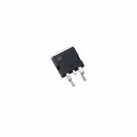
... VNB14N04 - VNK14N04FM - VNV14N04 4 Package information In order to meet environmental requirements, ST offers these devices in different grades of ® ECOPACK packages, depending on their level of environmental compliance. ECOPACK specifications, grade definitions and product status are available at: www.st.com. ® ECOPACK trademark. TO-263 (D2PAK) mechanical data Figure 30. ...
Page 14
... Package information Figure 31. SOT82-FM mechanical data 14/17 VNB14N04 - VNK14N04FM - VNV14N04 ...
Page 15
... VNB14N04 - VNK14N04FM - VNV14N04 Figure 32. PowerSO-10 mechanical data Package information 15/17 ...
Page 16
... Revision history 5 Revision history Table 5. Document revision history Date 20-Jan-1998 21-Jun-2004 08-Apr-2009 16/17 Revision 1 Initial release. 5 Update. Document reformatted. 6 Added Table 1: Device summary on page Updated Section 4: Package information on page 13 VNB14N04 - VNK14N04FM - VNV14N04 Changes 1. ...
Page 17
... VNB14N04 - VNK14N04FM - VNV14N04 Information in this document is provided solely in connection with ST products. STMicroelectronics NV and its subsidiaries (“ST”) reserve the right to make changes, corrections, modifications or improvements, to this document, and the products and services described herein at any time, without notice. All ST products are sold pursuant to ST’s terms and conditions of sale. ...