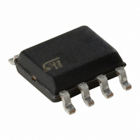
VNS1NV04D-E STMicroelectronics, VNS1NV04D-E Datasheet - Page 4

VNS1NV04D-E
Manufacturer Part Number
VNS1NV04D-E
Description
MOSFET 2N-CH 40V 1.7A 8-SOIC
Manufacturer
STMicroelectronics
Series
OMNIFET II™r
Type
Low Sider
Datasheet
1.VNS1NV04D13TR.pdf
(14 pages)
Specifications of VNS1NV04D-E
Input Type
Non-Inverting
Number Of Outputs
2
On-state Resistance
250 mOhm
Current - Peak Output
1.7A
Mounting Type
Surface Mount
Package / Case
8-SOIC (3.9mm Width)
Switch Type
Low Side
Power Switch Family
VNS1NV04D
Power Switch On Resistance
250mOhm
Output Current
2.6A
Mounting
Surface Mount
Package Type
SO
Operating Temperature (min)
-40C
Operating Temperature (max)
150C
Operating Temperature Classification
Automotive
Pin Count
8
Power Dissipation
4000W
Transistor Polarity
N-Channel
Resistance Drain-source Rds (on)
250 m Ohms
Drain-source Breakdown Voltage
40 V
Continuous Drain Current
1.7 A
Maximum Operating Temperature
+ 150 C
Mounting Style
SMD/SMT
Minimum Operating Temperature
- 40 C
Lead Free Status / RoHS Status
Lead free / RoHS Compliant
Voltage - Supply
-
Operating Temperature
-
Current - Output / Channel
-
Lead Free Status / Rohs Status
Compliant
Other names
497-5787-5
Available stocks
Company
Part Number
Manufacturer
Quantity
Price
VNS1NV04D
ELECTRICAL CHARACTERISTICS (continued) (T
DYNAMIC
SWITCHING
SOURCE DRAIN DIODE
PROTECTIONS (-40°C < T
(*) Pulsed: Pulse duration = 300 s, duty cycle 1.5%
4/14
2
Symbol
Symbol
(dI/dt)
Symbol
Symbol
V
g
C
t
t
t
t
I
SD
t
T
d(on)
d(off)
d(on)
d(off)
RRM
E
fs
T
Q
I
dlim
OSS
Q
I
t
lim
t
t
t
t
jsh
gf
rr
jrs
as
r
r
f
f
rr
(*)
i
(*)
on
Forward
Transconductance
Output Capacitance
Turn-on Delay Time
Rise Time
Turn-off Delay Time
Fall Time
Turn-on Delay Time
Rise Time
Turn-off Delay Time
Fall Time
Turn-on Current Slope
Total Input Charge
Forward On Voltage
Reverse Recovery Time
Reverse Recovery Charge
Reverse Recovery Current
Drain Current Limit
Step Response Current
Limit
Overtemperature
Shutdown
Overtemperature Reset
Fault Sink Current
Single Pulse
Avalanche Energy
Parameter
Parameter
Parameter
Parameter
j
< 150°C, unless otherwise specified)
V
V
V
V
(see figure 1)
V
V
(see figure 1)
V
V
V
I
I
I
V
(see test circuit, figure 2)
V
V
V
starting T
V
(see figures 3 & 4)
gen
SD
SD
DD
DS
DD
gen
DD
gen
DD
gen
DD
DD
IN
IN
IN
IN
=0.5A; V
=0.5A; dI/dt=6A/ s
=5V; V
=5V; V
=5V; V
=5V R
=13V; f=1MHz; V
=13V; I
=15V; I
=15V; I
=15V; I
=12V; I
=2.13mA (see figure 5)
=30V; L=200 H
=5V; R
=5V; R
=5V; R
j
=25°C; V
gen
DS
DS
DS
Test Conditions
D
Test Conditions
Test Conditions
Test Conditions
D
D
D
D
gen
gen
gen
IN
=0.5A
=0.5A
=0.5A
=1.5A
=0.5A; V
=13V
=13V
=13V; T
=R
=0V
=R
=2.2K
=R
IN MINn
j
IN MINn
IN MINn
=25°C, unless otherwise specified)
DD
j
IN
=T
IN
=24V
=330
=0V
=5V
=330
=330
jsh
L=50mH
Min
Min
Min
Min
150
135
1.7
10
55
Typ
0.25
0.75
Typ
Typ
Typ
170
200
205
100
175
350
0.8
2.0
1.3
1.8
1.2
5.0
5.0
90
70
15
2
1000
Max
Max
Max
Max
200
500
600
200
3.5
1.0
4.0
5.5
4.0
20
Unit
A/ s
Unit
Unit
Unit
mA
pF
mJ
nC
ns
°C
°C
ns
ns
ns
ns
S
V
A
A
C
s
s
s
s
s


