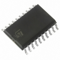
L9826 STMicroelectronics, L9826 Datasheet - Page 12

L9826
Manufacturer Part Number
L9826
Description
IC DRIVER OCTAL LOW SIDE SOIC-20
Manufacturer
STMicroelectronics
Type
Low Sider
Specifications of L9826
Input Type
SPI
Number Of Outputs
8
On-state Resistance
1.5 Ohm
Current - Peak Output
1.1A
Voltage - Supply
4.5 V ~ 5.5 V
Operating Temperature
-40°C ~ 150°C
Mounting Type
Surface Mount
Package / Case
20-SOIC (7.5mm Width)
Supply Voltage (min)
4.5 V
Supply Current
5 mA
Maximum Operating Temperature
+ 150 C
Mounting Style
SMD/SMT
Minimum Operating Temperature
- 40 C
Number Of Drivers
8
Lead Free Status / RoHS Status
Lead free / RoHS Compliant
Current - Output / Channel
-
Lead Free Status / Rohs Status
Lead free / RoHS Compliant
Available stocks
Company
Part Number
Manufacturer
Quantity
Price
Part Number:
L9826TR
Manufacturer:
ST
Quantity:
20 000
Functional description
5
5.1
5.2
5.2.1
12/19
Functional description
General
The L9826 is an 8-channel low-side driver assembled in SO20 package. Its 8-bit SPI serial
interface is designed to control all the outputs and to provide their diagnosis. Channels 1
and 2 are controlled either via SPI or via parallel through the inputs pins NON1 and NON2.
Diagnostic recognizes operative fault conditions: open load, short circuits to GND or to VB
and overcurrent.Thermal shutdown for outputs 1 and 2 is available as well the output voltage
clamp which is essential in case of working with inductive loads.
The reset feature is an OR function of the external reset nRes and the internal reset
generate during the undervoltage condition
Output stage control
Via parallel, only for output 1 and 2
This is valid only for Outputs 1 and 2 which are controlled through the dedicated inputs
NON1 and NON2 (both active low) which are internally configured as pull-up (see
This is to guarantee that the outputs are off in case of inputs open.
A further feature is the possibility to drive these outputs through a PWM signal
independently by SPI commands.
Reset signal is common for all the eight channels and it is active low. After an external reset
condition (that means NRES pin switched from low to high) to drive outputs 1 and 2 through
the parallel input (NON1 and NON2) it is necessary to disable the parallel input itself
(NON1, NON2 high) and then subsequently to drive the outputs 1 and 2 at the logic state
desiderated through NON1 and NON2. The duration of the command (T) as reported in the
Figure 4
In the next
scenario of parallel/series commands.
Figure 4.
Table 7.
SPI-bit 1, 2
Output 1, 2
NON1, 2
should be at less in the order of 100 nSecond.
Figure 4
Parallel control for output 1 and 2 (Example for Power-on)
Outputs control tables
off
1
0
is shown this behavior and in the next
Outputs 1, 2:
on
0
0
Doc ID 7214 Rev 9
on
0
1
on
1
1
SPI-bit 3 ... 8
Output 3 ... 8
Table 7
-
is summarized the
Outputs 3 to 8:
off
0
-
Figure
L9826
on
1
-
3).


