VND14NV04-E STMicroelectronics, VND14NV04-E Datasheet
VND14NV04-E
Specifications of VND14NV04-E
Available stocks


Related parts for VND14NV04-E


VND14NV04-E Summary of contents
Page 1
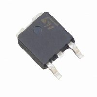
... MOSFETS KHz applications. Built-in thermal shutdown, linear current limitation and overvoltage clamp protect the chip in harsh environments. Fault feedback can be detected by monitoring the voltage at the input pin. Tube (lead free) VNB14NV04-E VNB14NV0413TR VND14NV04-E VND14NV0413TR VND14NV04-1-E - Doc ID 7393 Rev 8 "OMNIFET II" TO-252 (DPAK) ...
Page 2
... SO-8 thermal data . . . . . . . . . . . . . . . . . . . . . . . . . . . . . . . . . . . . . . . . . . 20 2 4.3 D PAK thermal data . . . . . . . . . . . . . . . . . . . . . . . . . . . . . . . . . . . . . . . . . 21 5 Package information . . . . . . . . . . . . . . . . . . . . . . . . . . . . . . . . . . . . . . . . 24 5.1 ECOPACK 5.2 TO-251 (IPAK) mechanical data . . . . . . . . . . . . . . . . . . . . . . . . . . . . . . . . 24 2 5.3 D PAK mechanical data . . . . . . . . . . . . . . . . . . . . . . . . . . . . . . . . . . . . . . 25 5.4 TO-252 (DPAK) mechanical data . . . . . . . . . . . . . . . . . . . . . . . . . . . . . . . 27 5.5 SO-8 mechanical data . . . . . . . . . . . . . . . . . . . . . . . . . . . . . . . . . . . . . . . 28 6 Revision history . . . . . . . . . . . . . . . . . . . . . . . . . . . . . . . . . . . . . . . . . . . 30 2/31 VNB14NV04, VND14NV04, VND14NV04-1, VNS14NV04 ® Doc ID 7393 Rev 8 ...
Page 3
... VNB14NV04, VND14NV04, VND14NV04-1, VNS14NV04 List of tables Table 1. Device summary . . . . . . . . . . . . . . . . . . . . . . . . . . . . . . . . . . . . . . . . . . . . . . . . . . . . . . . . . . 1 Table 2. Absolute maximum rating . . . . . . . . . . . . . . . . . . . . . . . . . . . . . . . . . . . . . . . . . . . . . . . . . . . 6 Table 3. Thermal data Table 4. Electrical characteristics . . . . . . . . . . . . . . . . . . . . . . . . . . . . . . . . . . . . . . . . . . . . . . . . . . . . 7 Table 5. DPAK thermal parameter . . . . . . . . . . . . . . . . . . . . . . . . . . . . . . . . . . . . . . . . . . . . . . . . . . 19 2 Table 6. D PAK thermal parameter . . . . . . . . . . . . . . . . . . . . . . . . . . . . . . . . . . . . . . . . . . . . . . . . . 22 Table 7. TO-251 (IPAK) mechanical data . . . . . . . . . . . . . . . . . . . . . . . . . . . . . . . . . . . . . . . . . . . . . 24 2 Table 8. D PAK mechanical data . . . . . . . . . . . . . . . . . . . . . . . . . . . . . . . . . . . . . . . . . . . . . . . . . . . 26 Table 9. ...
Page 4
... Figure 45. TO-252 (DPAK) package dimension . . . . . . . . . . . . . . . . . . . . . . . . . . . . . . . . . . . . . . . . . 27 Figure 46. SO-8 package dimension . . . . . . . . . . . . . . . . . . . . . . . . . . . . . . . . . . . . . . . . . . . . . . . . . . 28 4/31 VNB14NV04, VND14NV04, VND14NV04-1, VNS14NV04 . . . . . . . . . . . . . . . . . . . . . . . . . . . . . . . . . . . . . . . . . . . . . . . . . . . . . . . ( PAK ...
Page 5
... VNB14NV04, VND14NV04, VND14NV04-1, VNS14NV04 1 Block diagram Figure 1. Block diagram Doc ID 7393 Rev 8 Block diagram 5/31 ...
Page 6
... Total dissipation at T tot Maximum switching energy (L=0.4 mH MAX V =13 bat jstart T Operating junction temperature j T Case operating temperature c T Storage temperature stg 6/31 VNB14NV04, VND14NV04, VND14NV04-1, VNS14NV04 Parameter = =25 ° Ω; L =150 ° Doc ID 7393 Rev 8 Value 2 SO-8 DPAK IPAK D PAK ...
Page 7
... VNB14NV04, VND14NV04, VND14NV04-1, VNS14NV04 2.2 Thermal data Table 3. Thermal data Symbol Thermal resistance junction-case max R thj-case Thermal resistance junction-lead max R thj-lead Thermal resistance junction-ambient max R thj-amb 1. When mounted on a standard single-sided FR4 board with 0.5 cm pins. Horizontal mounting and no artificial air flow. ...
Page 8
... Step response current limit dlim T Over temperature shutdown jsh T Over temperature reset jrs I Fault sink current gf E Single pulse avalanche energy as 1. Pulsed: Pulse duration = 300 µs, duty cycle 1.5 % 8/31 VNB14NV04, VND14NV04, VND14NV04-1, VNS14NV04 Test Conditions 2.2 KΩ gen gen (see Figure 3) V ...
Page 9
... VNB14NV04, VND14NV04, VND14NV04-1, VNS14NV04 3 Protection features During normal operation, the input pin is electrically connected to the gate of the internal power MOSFET through a low impedance path. The device then behaves like a standard power MOSFET and can be used as a switch from KHz. The only difference from the user’s standpoint is that a small DC current I (typ. 100 µ ...
Page 10
... Protection features Figure 3. Switching time test circuit for resistive load Figure 4. Test circuit for diode recovery times 10/31 VNB14NV04, VND14NV04, VND14NV04-1, VNS14NV04 Doc ID 7393 Rev 8 ...
Page 11
... VNB14NV04, VND14NV04, VND14NV04-1, VNS14NV04 Figure 5. Unclamped inductive load test circuits Figure 7. Input charge test circuit Figure 6. Unclamped inductive waveforms Doc ID 7393 Rev 8 Protection features 11/31 ...
Page 12
... Protection features Figure 8. Source-drain diode forward characteristics Figure 10. Derating curve Figure 12. Static drain-source on resistance vs. input voltage (part 2/2) 12/31 VNB14NV04, VND14NV04, VND14NV04-1, VNS14NV04 Figure 9. Static drain source on resistance Figure 11. Static drain-source on resistance vs. input voltage (part 1/2) Figure 13. Transconductance Doc ID 7393 Rev 8 ...
Page 13
... VNB14NV04, VND14NV04, VND14NV04-1, VNS14NV04 Figure 14. Static drain-source on resistance vs. id Figure 16. Turn-on current slope (part 1/2) Figure 18. Input voltage vs. input charge Figure 15. Transfer characteristics Figure 17. Turn-on current slope (part 2/2) Figure 19. Turn-off drain source voltage slope (part 1/2) Doc ID 7393 Rev 8 Protection features ...
Page 14
... Protection features Figure 20. Turn-off drain source voltage slope (part 2/2) Figure 22. Switching time resistive load (part 1/2) Figure 24. Output characteristics 14/31 VNB14NV04, VND14NV04, VND14NV04-1, VNS14NV04 Figure 21. Capacitance variations Figure 23. Switching time resistive load (part 2/2) Figure 25. Normalized on resistance vs. temperature Doc ID 7393 Rev 8 ...
Page 15
... VNB14NV04, VND14NV04, VND14NV04-1, VNS14NV04 Figure 26. Normalized input threshold voltage vs. temperature Figure 28. Step response current limit Figure 27. Current limit vs. junction temperatures Doc ID 7393 Rev 8 Protection features 15/31 ...
Page 16
... V =13 Values are generated with R In case of repetitive pulses, T must not exceed the temperature specified above for curves B and C. Figure 30. DPAK demagnetization 16/31 VNB14NV04, VND14NV04, VND14NV04-1, VNS14NV04 =150ºC =100ºC Jstart =125ºC Jstart =0Ω L (at beginning of each demagnetization) of every pulse ...
Page 17
... VNB14NV04, VND14NV04, VND14NV04-1, VNS14NV04 2 Figure 31. D PAK maximum turn-off current versus load inductance Legend: A= Single pulse at T Jstart B= Repetitive pulse Repetitive pulse at T Conditions: V =13 Values are generated with R In case of repetitive pulses, T must not exceed the temperature specified above for curves B and C. ...
Page 18
... Package thermal data 4.1 DPAK thermal data Figure 33. DPAK PC board 1. Layout condition thickness=35 µm, Copper areas: from minimum pad lay-out Figure 34. DPAK R 18/31 VNB14NV04, VND14NV04, VND14NV04-1, VNS14NV04 (1) and Z measurements (PCB FR4 area = mm, PCB thickness=2 mm PCB copper area in open box free air condition thj-amb ...
Page 19
... VNB14NV04, VND14NV04, VND14NV04-1, VNS14NV04 Figure 35. DPAK thermal impedance junction ambient single pulse Figure 36. Thermal fitting model of an OMNIFET II in DPAK Pulse calculation formula δ ⋅ THδ TH δ T ⁄ where Table 5. DPAK thermal parameter Area/island(cm R1 (°C/W) R2 (°C/ °C/W) R4 (°C/W) R5 (°C/W) R6 (°C/W) C1 (W.s/°C) C2 (W.s/° ...
Page 20
... DPAK thermal parameter (continued) Area/island(cm C4 (W.s/°C) C5 (W.s/°C) C6 (W.s/°C) 4.2 SO-8 thermal data Figure 37. SO-8 PC board 1. Layout condition thickness=35 µm, Copper areas: 0.14 cm Figure 38. SO-8 R 20/31 VNB14NV04, VND14NV04, VND14NV04-1, VNS14NV04 2 ) Footprint 0.3 0.45 0.8 (1) and Z measurements (PCB FR4 area = mm, PCB thickness=2 mm ...
Page 21
... VNB14NV04, VND14NV04, VND14NV04-1, VNS14NV04 2 4.3 D PAK thermal data 2 Figure 39. D PAK PC board 1. Layout condition thickness=35 µm, Copper areas: from minimum pad lay-out Figure 40. D PAK R (1) and Z measurements (PCB FR4 area = mm, PCB thickness=2 mm PCB copper area in open box free air condition ...
Page 22
... THδ TH δ T ⁄ where = Table 6. D PAK thermal parameter Area/island(cm R1 (°C/W) R2 (°C/ °C/W) R4 (°C/W) R5 (°C/W) R6 (°C/W) C1 (W.s/°C) C2 (W.s/°C) 22/31 VNB14NV04, VND14NV04, VND14NV04-1, VNS14NV04 ( 1 δ – THtp 2 ) Footprint 0.1 0.35 0 0.0006 2.10E-03 Doc ID 7393 Rev 8 2 PAK 6 22 ...
Page 23
... VNB14NV04, VND14NV04, VND14NV04-1, VNS14NV04 2 Table 6. D PAK thermal parameter (continued) Area/island(cm C3 (W.s/°C) C4 (W.s/°C) C5 (W.s/°C) C6 (W.s/° Footprint 8.00E-02 0. Doc ID 7393 Rev 8 Package thermal data 6 5 23/31 ...
Page 24
... ECOPACK trademark. 5.2 TO-251 (IPAK) mechanical data TO-251 (IPAK) package dimension Figure 43. Table 7. TO-251 (IPAK) mechanical data Dim 24/31 VNB14NV04, VND14NV04, VND14NV04-1, VNS14NV04 Millimeters Min. Typ. 2.2 0.9 0.7 0.64 5.2 Doc ID 7393 Rev 8 ® Max. 2.4 1.1 1.3 0.9 ...
Page 25
... VNB14NV04, VND14NV04, VND14NV04-1, VNS14NV04 Table 7. TO-251 (IPAK) mechanical data (continued) Dim 5.3 D PAK mechanical data 2 Figure 44. D PAK package dimension Millimeters Min. Typ. 0.3 0.45 0.48 6 6.4 4.4 15.9 9 0.8 0.8 Doc ID 7393 Rev 8 Package information Max. 0.85 0.95 0.6 0.6 6 ...
Page 26
... Package information 2 Table 8. D PAK mechanical data Dim 26/31 VNB14NV04, VND14NV04, VND14NV04-1, VNS14NV04 Millimeters Min. Typ. 4.4 2.49 0.03 0.7 1.14 0.45 1.23 8. 8.5 4.88 15 1.27 1.4 2.4 0.4 0° Doc ID 7393 Rev 8 Max. 4.6 2.69 0.23 0.93 1.7 0.6 1.36 9 ...
Page 27
... VNB14NV04, VND14NV04, VND14NV04-1, VNS14NV04 5.4 TO-252 (DPAK) mechanical data Figure 45. TO-252 (DPAK) package dimension Table 9. TO-252 (DPAK) mechanical data Dim Millimeters Min. Typ. 2.20 0.90 0.03 0.64 5.20 0.45 0.48 6 5.1 6.4 4.7 2.28 4.4 9.35 0.8 Doc ID 7393 Rev 8 Package information Max ...
Page 28
... TO-252 (DPAK) mechanical data (continued) Dim Package weight 5.5 SO-8 mechanical data Figure 46. SO-8 package dimension Table 10. SO-8 mechanical data Dim 28/31 VNB14NV04, VND14NV04, VND14NV04-1, VNS14NV04 Millimeters Min. Typ. 0.6 0.2 0° 8° Gr. 0.29 Millimeters Min. Typ. 1.75 0.25 1.65 0.85 0.25 Doc ID 7393 Rev 8 Max ...
Page 29
... VNB14NV04, VND14NV04, VND14NV04-1, VNS14NV04 Table 10. SO-8 mechanical data (continued) Dim Millimeters Min. Typ. 0 6.2 1.27 3.81 4 1.27 0.6 Doc ID 7393 Rev 8 Package information Max. 0.25 4.8 5.8 3.8 0.4 8 29/31 ...
Page 30
... Revision history 6 Revision history Table 11. Document revision history Date 21-Jun-2004 03-Apr-2009 06-Apr-2010 30/31 VNB14NV04, VND14NV04, VND14NV04-1, VNS14NV04 Revision 6 Initial release. Document reformatted. 7 Added Table 1: Device summary on page Updated Section 5: Package information on page 24 Added part number VNS14NV04. Added SO-8 package: – Updated ...
Page 31
... VNB14NV04, VND14NV04, VND14NV04-1, VNS14NV04 Information in this document is provided solely in connection with ST products. STMicroelectronics NV and its subsidiaries (“ST”) reserve the right to make changes, corrections, modifications or improvements, to this document, and the products and services described herein at any time, without notice. All ST products are sold pursuant to ST’s terms and conditions of sale. ...