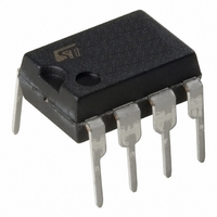
TDE1898RDP STMicroelectronics, TDE1898RDP Datasheet - Page 6

TDE1898RDP
Manufacturer Part Number
TDE1898RDP
Description
IC IPS HISIDE DRVR 0.5A 8-DIP
Manufacturer
STMicroelectronics
Type
High Sider
Datasheet
1.TDE1897RFPT.pdf
(12 pages)
Specifications of TDE1898RDP
Input Type
Differential
Number Of Outputs
1
Current - Output / Channel
500mA
Current - Peak Output
1.5A
Voltage - Supply
18 V ~ 35 V
Operating Temperature
-25°C ~ 85°C
Mounting Type
Through Hole
Package / Case
8-DIP (0.200", 5.08mm)
Lead Free Status / RoHS Status
Lead free / RoHS Compliant
On-state Resistance
-
Other names
497-5426-5
TDE1898RDP
TDE1898RDP
Available stocks
Company
Part Number
Manufacturer
Quantity
Price
Company:
Part Number:
TDE1898RDP
Manufacturer:
TE
Quantity:
1 200
Company:
Part Number:
TDE1898RDP
Manufacturer:
ST
Quantity:
5 510
TDE1897R - TDE1898R
WORST CONDITION POWER DISSIPATION IN
THE ON-STATE
In IPS applications the maximum average power
dissipation occurs when the device stays for a
long time in the ON state. In such a situation the
internal temperature depends on delivered cur-
rent (and related power), thermal characteristics
of the package and ambient temperature.
At ambient temperature close to upper limit
(+85°C) and in the worst operating conditions, it is
possible that the chip temperature could increase
so much to make the thermal shutdown proce-
dure untimely intervene.
Our aim is to find the maximum current the IPS
can withstand in the ON state without thermal
shutdown intervention, related to ambient tem-
perature. To this end, we should consider the fol-
lowing points:
1) The ON resistance R
2)
6/12
a) power lost in the switch:
b) power due to quiescent current in the ON
c) an external LED could be used to visualize
where:
NDMOS (the real switch) of the device in-
creases with its temperature.
Experimental results show that silicon resistiv-
ity increases with temperature at a constant
rate, rising of 60% from 25°C to 125°C.
The relationship between R
perature is therefore:
device is due to three contributes:
Thus the total ON state power consumption is
given by:
In the right side of equation 1, the second and
In the ON state the power dissipated in the
P
rent);
state Iq, sunk by the device in addition to
I
the switch state (OUTPUT STATUS pin).
Such a LED is driven by an internal current
source (delivering I
the voltage drop across the LED, the dissi-
pated power is: P
out
T
R
k is the constant rate (k
(see fig. 4).
P
out
j
DSON0
: P
R
is the silicon temperature in °C
on
DSON
q
I
out
P
is R
I
out
q
2
R
DSON
V
R
DSON0
P
s
DSON
(V
q
os
at T
os
s
) and therefore, if V
is the supply voltage);
P
(I
j
I
1
=25°C
out
os
DSON
os
is the output cur-
k
4.711
V
DSON
of the output
T
s
j
V
25
10
and tem-
(1)
os
3
.
)
os
is
3) The chip temperature must not exceed
Referring to application circuit in fig. 5, let us con-
sider the worst case:
- The supply voltage is at maximum value of in-
the third element are constant, while the first
one increases with temperature because
R
in order do not lose the control of the device.
The heat dissipation path is represented by
the thermal resistance of the system device-
board-ambient (R
tions, this parameter relates the power dissi-
pated P
the ambient temperature T
From this relationship, the maximum power P
which can be dissipated without exceeding
Replacing the expression (1) in this equation
and solving for I
current versus ambient temperature relation-
ship:
where R
course, I
maximum operative current I
nominal).
From the expression (2) we can also find the
maximum ambient temperature T
a given power P
In particular, this relation is useful to find the
maximum ambient temperature T
which I
dustrial bus (30V instead of the 24V nominal
value). This means also that I
T
DSON
Lim at a given ambient temperature T
I
T
Lim
outx
ambx
j
P
q
T
outx
increases as well.
T
on
amb
amb
outx
DSON
I
P
out
can be delivered:
P
to the silicon temperature T
Lim
os
on
2
values are top limited by the
P
x is R
Lim
on
out
R
on
Lim P
R
th
, we can find the maximum
can be dissipated:
DSONx
I
th
Lim T
R
). In steady state condi-
outx
R
th
R
T
DSON
th
R
2
amb
th
on
DSONx
amb
R
P
amb
R th
DSONx
at T
q
outx
:
P
q
P
outx
rises of 25%
amb
j
= Lim. Of
os
P
(4)
(2)
at which
ambx
amb
os
(500mA
R
j
is:
th
and
Lim
on
at


