MC33932VW Freescale Semiconductor, MC33932VW Datasheet - Page 3
MC33932VW
Manufacturer Part Number
MC33932VW
Description
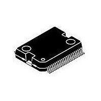
IC H-BRIDGE THROTTLE CTRL 44HSOP
Manufacturer
Freescale Semiconductor
Type
H Bridger
Datasheet
1.MC33932VW.pdf
(21 pages)
Specifications of MC33932VW
Input Type
Non-Inverting
Number Of Outputs
2
On-state Resistance
120 mOhm
Current - Output / Channel
5A
Current - Peak Output
11A
Voltage - Supply
8 V ~ 28 V
Operating Temperature
-40°C ~ 125°C
Mounting Type
Surface Mount
Package / Case
44-HSOP
Product
H-Bridge Drivers
Rise Time
3 us
Fall Time
3 us
Supply Voltage (max)
28 V
Supply Voltage (min)
- 0.3 V
Supply Current
80 uA
Maximum Operating Temperature
+ 125 C
Mounting Style
SMD/SMT
Bridge Type
H-Bridge
Maximum Turn-on Delay Time
1 ms
Minimum Operating Temperature
- 40 C
Number Of Drivers
4
Output Current
5 A
Output Voltage
7 V
Lead Free Status / RoHS Status
Lead free / RoHS Compliant
Available stocks
Company
Part Number
Manufacturer
Quantity
Price

Part Number:
MC33932VW
Manufacturer:
FRESSCAL
Quantity:
20 000


Table 1. 33932 Pin Definitions
Analog Integrated Circuit Device Data
Freescale Semiconductor
A functional description of each pin can be found in the Functional Description section beginning on
10,11,34,35
12,13,32,33
4-6,39,40
Pin
7-9
1
2
3
Pin Name
VPWRA
VPWRB
PGNDA
PGNDB
EN/D2
OUT1
FBA
D1
Power Input
Logic Input
Logic Input
Function
Ground
Ground
Analog
Output
Output
Power
Power
Power
Pin
VPWRA
VPWRA
VPWRA
VPWRB
VPWRB
PGNDA
PGNDA
PGNDB
PGNDB
EN/D2
CCPB
OUT1
OUT1
OUT1
OUT4
OUT4
OUT4
FBA
SFB
IN4
IN3
D1
H-Bridge Output 1
Disable Input 1
Positive Power
Power Ground
Power Ground
Formal Name
(Active High)
Enable Input
Feedback
Supply
1
2
3
4
5
6
7
8
9
10
11
12
13
14
15
16
17
18
19
20
21
22
Figure 3. 33932 Pin Connections
PIN CONNECTIONS
When D1 is logic HIGH, both OUT1 and OUT2 are tri-stated. Schmitt trigger
input with ~80 μA source so default condition = disabled.
H-Bridge A load current feedback output provides ground referenced 0.24% of
the high side output current. (Tie to GND through a resistor if not used.)
When EN/D2 is logic HIGH, H-Bridge A is operational. When EN/D2 is logic
LOW, the H-Bridge A outputs are tri-stated and H-bridge A is placed in Sleep
Mode. (logic input with ~ 80 μA sink so default condition = Sleep Mode.)
These pins must be connected together physically as close as possible and
directly soldered down to a wide, thick, low resistance supply plane on the PCB.
H-bridge A source of high side MOSFET1 and drain of low side MOSFET1.
High-current power ground pins must be connected together physically as
close as possible and directly soldered down to a wide, thick, low resistance
ground plane on the PCB.
High-current power ground pins must be connected together physically as
close as possible and directly soldered down to a wide, thick, low resistance
ground plane on the PCB.
H-BRIDGE A
H-BRIDGE B
AGNDB
AGNDA
Tab
Tab
44
43
42
41
40
39
38
37
36
35
34
33
32
31
30
29
28
27
26
25
24
23
Definition
SFA
IN1
IN2
CCPA
VPWRA
VPWRA
OUT2
OUT2
OUT2
PGNDA
PGNDA
PGNDB
PGNDB
OUT3
OUT3
OUT3
VPWRB
VPWRB
VPWRB
EN/D4
FBB
D3
page
11.
PIN CONNECTIONS
33932
3
Related parts for MC33932VW
Image
Part Number
Description
Manufacturer
Datasheet
Request
R

Part Number:
Description:
Manufacturer:
Freescale Semiconductor, Inc
Datasheet:
Part Number:
Description:
Manufacturer:
Freescale Semiconductor, Inc
Datasheet:
Part Number:
Description:
Manufacturer:
Freescale Semiconductor, Inc
Datasheet:
Part Number:
Description:
Manufacturer:
Freescale Semiconductor, Inc
Datasheet:
Part Number:
Description:
Manufacturer:
Freescale Semiconductor, Inc
Datasheet:
Part Number:
Description:
Manufacturer:
Freescale Semiconductor, Inc
Datasheet:
Part Number:
Description:
Manufacturer:
Freescale Semiconductor, Inc
Datasheet:
Part Number:
Description:
Manufacturer:
Freescale Semiconductor, Inc
Datasheet:
Part Number:
Description:
Manufacturer:
Freescale Semiconductor, Inc
Datasheet:
Part Number:
Description:
Manufacturer:
Freescale Semiconductor, Inc
Datasheet:
Part Number:
Description:
Manufacturer:
Freescale Semiconductor, Inc
Datasheet:
Part Number:
Description:
Manufacturer:
Freescale Semiconductor, Inc
Datasheet:
Part Number:
Description:
Manufacturer:
Freescale Semiconductor, Inc
Datasheet:
Part Number:
Description:
Manufacturer:
Freescale Semiconductor, Inc
Datasheet:
Part Number:
Description:
Manufacturer:
Freescale Semiconductor, Inc
Datasheet: