MC33932VW Freescale Semiconductor, MC33932VW Datasheet - Page 6
MC33932VW
Manufacturer Part Number
MC33932VW
Description
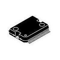
IC H-BRIDGE THROTTLE CTRL 44HSOP
Manufacturer
Freescale Semiconductor
Type
H Bridger
Datasheet
1.MC33932VW.pdf
(21 pages)
Specifications of MC33932VW
Input Type
Non-Inverting
Number Of Outputs
2
On-state Resistance
120 mOhm
Current - Output / Channel
5A
Current - Peak Output
11A
Voltage - Supply
8 V ~ 28 V
Operating Temperature
-40°C ~ 125°C
Mounting Type
Surface Mount
Package / Case
44-HSOP
Product
H-Bridge Drivers
Rise Time
3 us
Fall Time
3 us
Supply Voltage (max)
28 V
Supply Voltage (min)
- 0.3 V
Supply Current
80 uA
Maximum Operating Temperature
+ 125 C
Mounting Style
SMD/SMT
Bridge Type
H-Bridge
Maximum Turn-on Delay Time
1 ms
Minimum Operating Temperature
- 40 C
Number Of Drivers
4
Output Current
5 A
Output Voltage
7 V
Lead Free Status / RoHS Status
Lead free / RoHS Compliant
Available stocks
Company
Part Number
Manufacturer
Quantity
Price

Part Number:
MC33932VW
Manufacturer:
FRESSCAL
Quantity:
20 000


Table 3. Static Electrical Characteristics
values noted reflect the approximate parameter means at T
Specifications given for H-Bridge A apply symmetrically to H-Bridge B.
6
33932
ELECTRICAL CHARACTERISTICS
STATIC ELECTRICAL CHARACTERISTICS
POWER INPUTS (VPWR)
CHARGE PUMP
CONTROL INPUTS
Notes
Operating Voltage Range
Sleep State Supply Current
Standby Supply Current (Part Enabled)
Under-voltage Lockout Thresholds
Charge Pump Voltage (CP Capacitor = 33 nF), No PWM
Charge Pump Voltage (CP Capacitor = 33 nF), PWM = 11 kHz
Operating Input Voltage (IN1, IN2, D1, EN/D2, IN3, IN4, D3, EN/D4)
Input Voltage (IN1, IN2, D1, EN/D2, IN3, IN4, D3, EN/D4)
Logic Input Currents, VPWR = 8.0 V
10.
11.
12.
Characteristics noted under conditions 8.0 V ≤ V
Steady-state
Transient (t < 500 ms)
Quasi-Functional (R
EN/
I
V
V
Hysteresis
V
V
V
V
Logic Threshold HIGH
Logic Threshold LOW
Hysteresis
Input EN/D2, EN/D4 (internal pull-downs), V
Inputs IN1, IN2, D1, IN3, IN4, D3 (internal pull-ups), VIL = 0 V
OUT
PWR(falling)
PWR(rising)
PWR
PWR
PWR
PWR
Device specifications are characterized over the range of 8.0 V ≤ V
reliability. Device is operational down to 5.0V, but below 8.0 V the output resistance may increase by 50 percent.
Device will survive the transient over-voltage indicated for a maximum duration of 500 ms. Transient not to be repeated more than once
every 10 seconds.
I
D2
PWR(SLEEP)
= 0 A, V
= 5.0 V
= 28 V
= 5.0 V
= 28 V
= Logic [0], IN1, IN2, D1 = Logic [1], and I
EN
is with Sleep Mode activated and EN/
= 5.0 V
DS(ON)
(11)
(10)
(12)
Characteristic
May Increase by 50%)
STATIC ELECTRICAL CHARACTERISTICS
IH
= 5.0 V
OUT
PWR
= 0 A
D2
≤ 28 V, - 40°C ≤ T
, = logic [0], and IN1, IN2, D1 = logic [1] or with these inputs left floating.
A
= 25°C under nominal conditions, unless otherwise noted.
V
PWR
I
V
PWR(STANDBY)
UVLO(INACTIVE)
I
V
UVLO(ACTIVE)
V
V
PWR(SLEEP)
V
V
UVLO(HYS)
CP
CP
Symbol
V
PWR(SS)
PWR(QF)
≤ 28 V. Continuous operation above 28 V may degrade device
V
PWR(t)
A
V
V
- V
- V
I
HYS
V
IN
IH
IL
≤ 125°C, GND = 0 V, unless otherwise noted. Typical
I
PWR
PWR
-200
4.15
Min
150
250
8.0
5.0
3.5
3.5
2.0
20
–
–
–
–
–
–
–
–
Analog Integrated Circuit Device Data
Typ
200
400
-80
80
–
–
–
–
–
–
–
–
–
–
–
–
–
–
Freescale Semiconductor
Max
350
200
8.0
5.0
5.5
1.0
-20
28
40
50
20
12
12
–
–
–
–
–
Unit
mA
mV
mV
μA
μA
V
V
V
V
V
V
V
V
Related parts for MC33932VW
Image
Part Number
Description
Manufacturer
Datasheet
Request
R

Part Number:
Description:
Manufacturer:
Freescale Semiconductor, Inc
Datasheet:
Part Number:
Description:
Manufacturer:
Freescale Semiconductor, Inc
Datasheet:
Part Number:
Description:
Manufacturer:
Freescale Semiconductor, Inc
Datasheet:
Part Number:
Description:
Manufacturer:
Freescale Semiconductor, Inc
Datasheet:
Part Number:
Description:
Manufacturer:
Freescale Semiconductor, Inc
Datasheet:
Part Number:
Description:
Manufacturer:
Freescale Semiconductor, Inc
Datasheet:
Part Number:
Description:
Manufacturer:
Freescale Semiconductor, Inc
Datasheet:
Part Number:
Description:
Manufacturer:
Freescale Semiconductor, Inc
Datasheet:
Part Number:
Description:
Manufacturer:
Freescale Semiconductor, Inc
Datasheet:
Part Number:
Description:
Manufacturer:
Freescale Semiconductor, Inc
Datasheet:
Part Number:
Description:
Manufacturer:
Freescale Semiconductor, Inc
Datasheet:
Part Number:
Description:
Manufacturer:
Freescale Semiconductor, Inc
Datasheet:
Part Number:
Description:
Manufacturer:
Freescale Semiconductor, Inc
Datasheet:
Part Number:
Description:
Manufacturer:
Freescale Semiconductor, Inc
Datasheet:
Part Number:
Description:
Manufacturer:
Freescale Semiconductor, Inc
Datasheet: