MC33932VW Freescale Semiconductor, MC33932VW Datasheet - Page 5
MC33932VW
Manufacturer Part Number
MC33932VW
Description
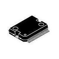
IC H-BRIDGE THROTTLE CTRL 44HSOP
Manufacturer
Freescale Semiconductor
Type
H Bridger
Datasheet
1.MC33932VW.pdf
(21 pages)
Specifications of MC33932VW
Input Type
Non-Inverting
Number Of Outputs
2
On-state Resistance
120 mOhm
Current - Output / Channel
5A
Current - Peak Output
11A
Voltage - Supply
8 V ~ 28 V
Operating Temperature
-40°C ~ 125°C
Mounting Type
Surface Mount
Package / Case
44-HSOP
Product
H-Bridge Drivers
Rise Time
3 us
Fall Time
3 us
Supply Voltage (max)
28 V
Supply Voltage (min)
- 0.3 V
Supply Current
80 uA
Maximum Operating Temperature
+ 125 C
Mounting Style
SMD/SMT
Bridge Type
H-Bridge
Maximum Turn-on Delay Time
1 ms
Minimum Operating Temperature
- 40 C
Number Of Drivers
4
Output Current
5 A
Output Voltage
7 V
Lead Free Status / RoHS Status
Lead free / RoHS Compliant
Available stocks
Company
Part Number
Manufacturer
Quantity
Price

Part Number:
MC33932VW
Manufacturer:
FRESSCAL
Quantity:
20 000


Table 2. Maximum Ratings
permanent damage to the device. These parameters are not production tested.
Analog Integrated Circuit Device Data
Freescale Semiconductor
ELECTRICAL RATINGS
THERMAL RATINGS
Notes
Power Supply Voltage
Logic Input Voltage
SFA
Continuous Output Current
ESD Voltage
Storage Temperature
Operating Temperature
Peak Package Reflow Temperature During Reflow
Approximate Junction-to Case Thermal Resistance
All voltages are with respect to ground unless otherwise noted. Exceeding these ratings may cause a malfunction or
1.
2.
3.
4.
5.
6.
7.
8.
9.
Normal Operation (Steady-state)
Transient Overvoltage
Human Body Model
Machine Model
Charge Device Model
Ambient
Junction
,
SFB
Device will survive repetitive transient over-voltage conditions for durations not to exceed 500ms
External protection is required to prevent device damage in case of a reverse battery condition.
Exceeding the maximum input voltage on IN1, IN2, IN3, IN4, EN/D2, EN/D4, D1, or D3 may cause a malfunction or permanent damage
to the device.
Exceeding the pull-up resistor voltage on the open drain
Continuous output current capability is dependent on sufficient package heatsinking to keep junction temperature ≤ 150
ESD testing is performed in accordance with the Human Body Model (C
R
The limiting factor is junction temperature, taking into account the power dissipation, thermal resistance, and heat sinking provided. Brief
non-repetitive excursions of junction temperature above 150
maximum. (Non-repetitive events are defined as not occurring more than once in 24 hours.)
Pin soldering temperature limit is for 10 seconds maximum duration. Not designed for immersion soldering. Exceeding these limits may
cause malfunction or permanent damage to the device.
Freescale’s Package Reflow capability meets Pb-free requirements for JEDEC standard J-STD-020C. For Peak Package Reflow
Temperature and Moisture Sensitivity Levels (MSL), Go to www.freescale.com, search by part number [e.g. remove prefixes/suffixes
and enter the core ID to view all orderable parts. (i.e. MC33xxxD enter 33xxx), and review parametrics.
Exposed heatsink pad plus the power and ground pins comprise the main heat conduction paths. The actual R
values will vary depending on solder thickness and composition and copper trace thickness and area. Maximum current at maximum
die temperature represents ~16 W of conduction loss heating in the diagonal pair of output MOSFETs. Therefore, the RθJA must be
< 5.0°C/W for maximum current at 70°C ambient. Module thermal design must be planned accordingly.
ZAP
Corner Pins (1,9,17,25)
All Other Pins
Output
= 0 Ω), and the Charge Device Model (CDM), Robotic (C
(5)
(3)
(2)
(6)
(1)
(4)
Ratings
ELECTRICAL CHARACTERISTICS
(7),
(9)
(8)
MAXIMUM RATINGS
SFA
°
C can be tolerated, provided the duration does not exceed 30 seconds
or
ZAP
SFB
= 4.0 pF).
pin may cause permanent damage to the device.
ZAP
= 100 pF, R
I
V
OUT(CONT)
V
Symbol
PWR(SS)
V
V
R
T
PWR(T)
T
V
V
ESD1
ESD2
PPRT
THJC
T
STG
T
SF
IN
A
J
ZAP
= 1500 Ω), Machine Model (C
@
ELECTRICAL CHARACTERISTICS
duty cycle not to exceed 10%.
- 0.3 to 7.0
- 0.3 to 7.0
- 65 to 150
- 40 to 125
- 40 to 150
- 0.3 to 28
- 0.3 to 40
± 2000
Value
Note 8
± 200
±750
±500
<1.0
5.0
θJB
(junction-to-PC board)
MAXIMUM RATINGS
°
C.
ZAP
°
= 200 pF,
Unit
C/W
°
°
°C
V
V
V
A
V
C
C
33932
5
Related parts for MC33932VW
Image
Part Number
Description
Manufacturer
Datasheet
Request
R

Part Number:
Description:
Manufacturer:
Freescale Semiconductor, Inc
Datasheet:
Part Number:
Description:
Manufacturer:
Freescale Semiconductor, Inc
Datasheet:
Part Number:
Description:
Manufacturer:
Freescale Semiconductor, Inc
Datasheet:
Part Number:
Description:
Manufacturer:
Freescale Semiconductor, Inc
Datasheet:
Part Number:
Description:
Manufacturer:
Freescale Semiconductor, Inc
Datasheet:
Part Number:
Description:
Manufacturer:
Freescale Semiconductor, Inc
Datasheet:
Part Number:
Description:
Manufacturer:
Freescale Semiconductor, Inc
Datasheet:
Part Number:
Description:
Manufacturer:
Freescale Semiconductor, Inc
Datasheet:
Part Number:
Description:
Manufacturer:
Freescale Semiconductor, Inc
Datasheet:
Part Number:
Description:
Manufacturer:
Freescale Semiconductor, Inc
Datasheet:
Part Number:
Description:
Manufacturer:
Freescale Semiconductor, Inc
Datasheet:
Part Number:
Description:
Manufacturer:
Freescale Semiconductor, Inc
Datasheet:
Part Number:
Description:
Manufacturer:
Freescale Semiconductor, Inc
Datasheet:
Part Number:
Description:
Manufacturer:
Freescale Semiconductor, Inc
Datasheet:
Part Number:
Description:
Manufacturer:
Freescale Semiconductor, Inc
Datasheet: