VN340SP-E STMicroelectronics, VN340SP-E Datasheet - Page 5
VN340SP-E
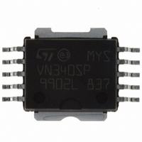
Manufacturer Part Number
VN340SP-E
Description
IC DRIVER QUAD 0.7A POWERSO-10
Manufacturer
STMicroelectronics
Type
High Sider
Datasheet
1.VN340SPTR-E.pdf
(16 pages)
Specifications of VN340SP-E
Input Type
Non-Inverting
Number Of Outputs
4
On-state Resistance
200 mOhm
Current - Output / Channel
700mA
Current - Peak Output
4A
Voltage - Supply
10 V ~ 36 V
Mounting Type
Surface Mount
Package / Case
PowerSO-10 Exposed Bottom Pad
Control Voltage Range
10 V to 36 V
Load Voltage Rating
36 V
Load Current Rating
0.7 A
Mounting Style
SMD/SMT
Relay Type
Solid State
Termination Style
Surface Mount
Current, Output
0.7 A @ 85 °C
Package Type
SO-10
Temperature, Ambient, Minimum
-55 °C
Temperature, Range, Operating Ambient
-55 °C
Thermal Resistance, Junction To Ambient
50 °C⁄W
Time, Rise, Turn-on
52 us (Typ.)
Transistor Type
IGBT
Voltage, Output, High Level
3.5 V
Voltage, Supply
36 V
For Use With
497-6261 - BOARD EVAL CENTRAL UNIT ALARM497-5511 - EVAL BOARD FOR 4CH HI SIDE DRVR
Lead Free Status / RoHS Status
Lead free / RoHS Compliant
Operating Temperature
-
Lead Free Status / Rohs Status
Lead free / RoHS Compliant
Other names
497-5053-5
Available stocks
Company
Part Number
Manufacturer
Quantity
Price


VN340SP-E
3
Table 3.
Table 4.
Table 5.
1. The input voltage is internally clamped at 32V minimum, it is possible to connect the input pins to an higher voltage via an
Symbol
V
Symbol
Symbol
V
t
I(HYST)
I
t
external resistor calculate to not exceed 10mA
d(OFF)
V
R
LGND
V
V
demag
d(ON)
V
V
I
ICL
I
IN
CC
ON
t
IH
OL
t
IL
S
r
f
Electrical characteristics
10V < V
I/O Input low level voltage
I/O Input high level
voltage
I/O Input hysteresis
voltage
I/O Input current
I/O Input clamp voltage
Supply voltage
On state resistance
Supply current
Low state output voltage V
Output voltage at turn-off I
Output current at turn-off
Logical input
Power section
Switching ( V
Turn-on delay time of
Output current
Rise time of output
current
Turn-off delay time of
output current
Fall time of output
current
CC
Parameter
(1)
Parameter
Parameter
< 36V; -40°C < T
CC
= 24V)
(1)
I
I
I
All channels OFF
On state; V
(T
V
Tamb = - 25°C to 85°C
I
time < 0.1µs, T
I
time < 0.1µs, T
I
time < 0.1µs, T
I
time < 0.1µs, T
V
I
I
OUT
OUT
OUT
OUT
OUT
OUT
OUT
OUT
IN
IN
IN
CC
IN
J
J
= 1mA
= -1mA
= 125°C)
< 125°C; unless otherwise specified
= V
= 30V
= V
= 0.5A; T
= 0.5A; T
= 0.5A; T
= 0.5A; L
= 0.5A, resistive load input rise
= 0.5A, resistive load input rise
= 0.5A, resistive load input rise
= 0.5A, resistive load input rise
IL
INn
; R
Test conditions
IN
Test conditions
= V
LOAD
Test conditions
= 30V; I
LOAD
J
J
J
GND
J
J
J
J
= 25°C
= 85°C
= 125°C
= 25°C
= 25°C
= 25°C
= 25°C
>= 10MΩ
= V
>= 1mH
OUT
STAT
Figure 6.
= 0V
= 18 to 30V
V
Min
CC
Min
Min
10
3.5
32
-65 V
CC
Typ
Electrical characteristics
Typ
52
94
34
Typ
-0.7
8
0.5
36
-55 V
Max
0.32
CC
Max
100
250
0.2
0.4
1.5
Max
36
50
20
1
6
2
25
2
-45
Unit
Unit
mA
mA
mA
Unit
Ω
Ω
Ω
µs
µs
µs
µs
V
V
V
µΑ
V
V
V
V
V
5/16
Related parts for VN340SP-E
Image
Part Number
Description
Manufacturer
Datasheet
Request
R

Part Number:
Description:
STMicroelectronics [RIPPLE-CARRY BINARY COUNTER/DIVIDERS]
Manufacturer:
STMicroelectronics
Datasheet:
Part Number:
Description:
STMicroelectronics [LIQUID-CRYSTAL DISPLAY DRIVERS]
Manufacturer:
STMicroelectronics
Datasheet:

Part Number:
Description:
BOARD EVAL FOR MEMS SENSORS
Manufacturer:
STMicroelectronics
Datasheet:
Part Number:
Description:
NPN TRANSISTOR POWER MODULE
Manufacturer:
STMicroelectronics
Datasheet:
Part Number:
Description:
TURBOSWITCH ULTRA-FAST HIGH VOLTAGE DIODE
Manufacturer:
STMicroelectronics
Datasheet:
Part Number:
Description:
Manufacturer:
STMicroelectronics
Datasheet:
Part Number:
Description:
DIODE / SCR MODULE
Manufacturer:
STMicroelectronics
Datasheet:
Part Number:
Description:
DIODE / SCR MODULE
Manufacturer:
STMicroelectronics
Datasheet:
Part Number:
Description:
Search -----> STE16N100
Manufacturer:
STMicroelectronics
Datasheet:
Part Number:
Description:
Search ---> STE53NA50
Manufacturer:
STMicroelectronics
Datasheet:
Part Number:
Description:
NPN Transistor Power Module
Manufacturer:
STMicroelectronics
Datasheet:
Part Number:
Description:
DIODE / SCR MODULE
Manufacturer:
STMicroelectronics
Datasheet: