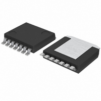
BD6231HFP-TR Rohm Semiconductor, BD6231HFP-TR Datasheet - Page 11

BD6231HFP-TR
Manufacturer Part Number
BD6231HFP-TR
Description
IC H-BRIDGE DVR 36V 1CH 1A HRP7
Manufacturer
Rohm Semiconductor
Series
-r
Type
Half Bridge Driverr
Datasheet
1.BD6230HFP-TR.pdf
(17 pages)
Specifications of BD6231HFP-TR
Applications
DC Motor Driver
Number Of Outputs
1
Current - Output
1A
Voltage - Supply
6 V ~ 32 V
Operating Temperature
-40°C ~ 85°C
Mounting Type
Surface Mount
Package / Case
HRP-7
Evaluation Tools
-
Voltage - Load
-
Product
H-Bridge Drivers
Supply Voltage (max)
36 V
Supply Voltage (min)
6 V
Supply Current
1.3 mA
Maximum Power Dissipation
1.4 W
Maximum Operating Temperature
+ 85 C
Mounting Style
SMD/SMT
Bridge Type
H-bridge
Minimum Operating Temperature
- 40 C
Number Of Drivers
1
Output Current
1 A
Operating Supply Voltage
6 V to 32 V
Lead Free Status / RoHS Status
Lead free / RoHS Compliant
Voltage - Load
-
Lead Free Status / Rohs Status
Lead free / RoHS Compliant
Available stocks
Company
Part Number
Manufacturer
Quantity
Price
Company:
Part Number:
BD6231HFP-TR
Manufacturer:
ROHM Semiconductor
Quantity:
3 984
Company:
Part Number:
BD6231HFP-TR
Manufacturer:
ROHM
Quantity:
469
Part Number:
BD6231HFP-TR
Manufacturer:
ROHM/罗姆
Quantity:
20 000
○
BD6230, BD6231, BD6232, BD6235, BD6236, BD6237
c
www.rohm.com
2009 ROHM Co., Ltd. All rights reserved.
2) Cross-conduction protection circuit
3) Output protection circuits
i) j) VREF control mode
In the full bridge output stage, when the upper and lower transistors are turned on at the same time, and this condition
exists during the period of transition from high to low, or low to high, a rush current flows from the power supply to
ground, resulting in a loss. This circuit protects against the rush current by providing a dead time (about 400ns,
nominal) at the transition.
a) Under voltage lock out (UVLO) circuit
b) Over voltage protection (OVP) circuit
The built-in VREF-switching on duty conversion circuit provides switching duty corresponding to the voltage of the
VREF pin and the VCC voltage. The function offers the same level of control as the high voltage output setting
function in previous models. The on duty is shown by the following equation.
DUTY ≈ VREF [V] / VCC [V]
For example, if VCC voltage is 24V and VREF pin voltage is 18V, the switching on duty is about 75 percent.
However, please note that the switching on duty might be limited by the range of VREF pin voltage (Refer to the
operating conditions, shown on page 2). The PWM carrier frequency in this mode is 25kHz (nominal), and the
switching operation is the same as it is the PWM control modes. When operating in this mode, do not input the
PWM signal to the FIN and RIN pins. In addition, establish a current path for the recovery current from the motor, by
connecting a bypass capacitor (10µF or more is recommended) between VCC and ground.
To secure the lowest power supply voltage necessary to operate the controller, and to prevent under voltage
malfunctions, a UVLO circuit has been built into this driver. When the power supply voltage falls to 5.0V (nominal) or
below, the controller forces all driver outputs to high impedance. When the voltage rises to 5.5V (nominal) or above,
the UVLO circuit ends the lockout operation and returns the chip to normal operation.
When the power supply voltage exceeds 45V (nominal), the controller forces all driver outputs to high impedance.
The OVP circuit is released and its operation ends when the voltage drops back to 40V (nominal) or below. This
protection circuit does not work in the stand-by mode. Also, note that this circuit is supplementary, and thus if it is
asserted, the absolute maximum rating will have been exceeded. Therefore, do not continue to use the IC after this
circuit is activated, and do not operate the IC in an environment where activation of the circuit is assumed.
VREF
OUT1
OUT2
VCC
RIN
FIN
0
Fig.42 VREF control operation (timing chart)
11/16
2009.08 - Rev.C
Technical Note


