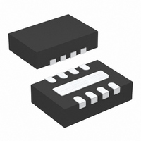
LTC4354IDDB#TRPBF Linear Technology, LTC4354IDDB#TRPBF Datasheet - Page 5

LTC4354IDDB#TRPBF
Manufacturer Part Number
LTC4354IDDB#TRPBF
Description
IC MON DIODE-OR CTRLR NEG 8DFN
Manufacturer
Linear Technology
Datasheet
1.LTC4354CS8PBF.pdf
(12 pages)
Specifications of LTC4354IDDB#TRPBF
Applications
-48V Dist Power Systems, AdvancedTCA ® Systems
Fet Type
N-Channel
Number Of Outputs
2
Internal Switch(s)
No
Delay Time - Off
700ns
Voltage - Supply
4.5 V ~ 11.75 V
Current - Supply
1.2mA
Operating Temperature
-40°C ~ 85°C
Mounting Type
Surface Mount
Package / Case
8-DFN
Lead Free Status / RoHS Status
Lead free / RoHS Compliant
Delay Time - On
-
Available stocks
Company
Part Number
Manufacturer
Quantity
Price
PI FU CTIO S
DA, DB (Pins 1, 8): Drain Voltage Sense Inputs. These
pins sense source-drain voltage drop across the N-Chan-
nel MOSFETs. An external resistor is recommended to
protect these pins from transient voltages exceeding 80V
in extreme fault conditions. For Kelvin sensing, connect
these pins as close to the drains as possible. Connect to
V
V
pin to the positive side of the supply through a resistor. An
internal shunt regulator that can sink up to 20mA typically
clamps V
V
GA, GB (Pins 4, 6): Gate Drive Outputs. Gate pins pull high
to 10V minimum, fully enhancing the N-Channel MOSFET,
when the load current creates more than 30mV of drop
across the FET. When the load current is small, the gates
are actively servoed to maintain a 30mV drop across the
MOSFET. If reverse current develops more than –140mV
of voltage drop across the MOSFET, the pins pull low to
V
FU CTIO AL DIAGRA
SS
CC
SS
SS
U
.
U
if unused.
in less than 1µs. Quickly turning off the pass transis-
(Pin 3): Positive Supply Voltage Input. Connect this
CC
U
at 11V. Bypass this pin with a 1µF capacitor to
U
U
W
FAULT
7
+
–
3
V
V
SS
CC
BV = 11V
30mV
V
V
SS
SS
+
–
30mV
FAULT DETECTION
tors prevents excessive reverse currents. Leave the pins
open if unused.
V
device negative supply input and connects to the common
source connection of the N-Channel MOSFETs. It also
connects to the source voltage sense input of the servo
amplifiers. For Kelvin sensing, connect pin 5 as close to
the common source terminal of the MOSFETs as possible.
FAULT (Pin 7): Fault Output. Open drain output that
normally pulls the FAULT pin to V
turn off an external LED or optocoupler. In the fault
condition, where the pass transistor is fully on and the
voltage drop across it is higher than the fault threshold, the
FAULT pin goes high impedance, turning on the LED or
optocoupler. This indicates that one or both of the pass
transistors have failed open or failed short creating a cross
conduction current in between the two power supplies.
Connect to V
EXPOSED PAD (Pin 9): Exposed pad is common to V
and may be left open or connected to pins 2 and 5.
SS
–
–
+
+
AMP A
AMP B
(Pins 2, 5): Negative Supply Voltage Input. This is the
55k
55k
4354 FD01
SS
5
4
1
6
8
2
V
GA
DA
GB
DB
V
if unused.
SS
SS
SS
and shunts current to
LTC4354
4354fb
5
SS


