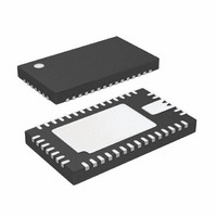
LTC3577EUFF#PBF Linear Technology, LTC3577EUFF#PBF Datasheet - Page 33

LTC3577EUFF#PBF
Manufacturer Part Number
LTC3577EUFF#PBF
Description
IC PWR MANAGEMENT HANDHELD 44QFN
Manufacturer
Linear Technology
Datasheet
1.LTC3577EUFFPBF.pdf
(54 pages)
Specifications of LTC3577EUFF#PBF
Applications
Handheld/Mobile Devices
Voltage - Supply
4.35 V ~ 5.5 V
Operating Temperature
-40°C ~ 85°C
Mounting Type
Surface Mount
Package / Case
44-QFN
Lead Free Status / RoHS Status
Lead free / RoHS Compliant
Current - Supply
-
Available stocks
Company
Part Number
Manufacturer
Quantity
Price
OPERATION
increases until it is turned on continuously at 100%. In this
dropout condition, the respective output voltage equals the
regulator’s input voltage minus the voltage drops across
the internal P-channel MOSFET and the inductor.
Soft-Start Operation
Soft-start is accomplished by gradually increasing the peak
inductor current for each step-down switching regulator
over a 500μs period. This allows each output to rise slowly,
helping minimize inrush current required to charge up the
switching regulator output capacitor. A soft-start cycle
occurs whenever a given switching regulator is enabled.
A soft-start cycle is not triggered by changing operating
modes. This allows seamless output transition when
actively changing between operating modes.
Slew Rate Control
The step-down switching regulators contain new patent
pending circuitry to limit the slew rate of the switch node
(SW1, SW2 and SW3). This new circuitry is designed to
transition the switch node over a period of a few nanosec-
onds, signifi cantly reducing radiated EMI and conducted
supply noise while maintaining high effi ciency. Since
slowing the slew rate of the switch nodes causes effi ciency
loss, the slew rate of the step-down switching regulators is
adjustable via the I
This allows the user to optimize effi ciency or EMI as neces-
sary with four different slew rate settings. The power-up
default is the fastest slew rate (highest effi ciency) setting.
Figure 14. V
100
1.00E-05
90
80
70
60
50
40
30
20
10
0
OUT3
2
(1.2V) Effi ciency and Power Loss vs I
C registers SLEWCTL1 and SLEWCTL2.
1.00E-0.3
I
OUT3
(mA)
Burst Mode
OPERATION
V
SW[1:0] =
1.00E-01
IN
= 3.8V
3577 F14
00
01
10
11
1.00E+00
1.00e-01
1.00E-02
1.00E-03
1.00E-04
1.00E-05
OUT3
Figures 14 and 15 show the effi ciency and power loss
graph for Buck3 programmed for 1.2V and 2.5V outputs.
Note that the power loss curves remain fairly constant for
both graphs yet changing the slew rate has a larger effect
on the 1.2V output effi ciency. This is mainly because for
a given output current the 2.5V output is delivering more
than 2x the power than the 1.2V output. Effi ciency will
always decrease and show more variation to slew rate as
the programmed output voltage is decreased.
Low Supply Operation
An undervoltage lockout circuit on V
shuts down the step-down switching regulators when V
drops below about 2.7V. It is recommended that the step-
down switching regulator input supplies (V
connected to the power path output (V
UVLO prevents the step-down switching regulators from
operating at low supply voltages where loss of regula-
tion or other undesirable operation may occur. If driving
the step-down switching regulator input supplies from
a voltage other than the V
not be operated outside the specifi ed operating range as
operation is not guaranteed beyond this range.
Inductor Selection
Many different sizes and shapes of inductors are available
from numerous manufacturers. Choosing the right inductor
from such a large selection of devices can be overwhelming,
but following a few basic guidelines will make the selection
Figure 15. V
100
1.00E-05
90
80
70
60
50
40
30
20
10
0
OUT3
LTC3577/LTC3577-1
(2.5V) Effi ciency and Power Loss vs I
1.00E-0.3
I
OUT3
OUT
(mA)
pin, the regulators should
Burst Mode
OPERATION
V
SW[1:0] =
1.00E-01
IN
= 3.8V
OUT
OUT
3577 F15
00
01
10
11
) directly. This
(V
IN12
1.00E+00
1.00e-01
1.00E-02
1.00E-03
1.00E-04
1.00E-05
OUT
, V
33
UVLO)
IN3
OUT3
3577fa
) be
OUT


