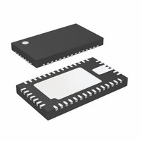
LTC3577EUFF#PBF Linear Technology, LTC3577EUFF#PBF Datasheet - Page 46

LTC3577EUFF#PBF
Manufacturer Part Number
LTC3577EUFF#PBF
Description
IC PWR MANAGEMENT HANDHELD 44QFN
Manufacturer
Linear Technology
Datasheet
1.LTC3577EUFFPBF.pdf
(54 pages)
Specifications of LTC3577EUFF#PBF
Applications
Handheld/Mobile Devices
Voltage - Supply
4.35 V ~ 5.5 V
Operating Temperature
-40°C ~ 85°C
Mounting Type
Surface Mount
Package / Case
44-QFN
Lead Free Status / RoHS Status
Lead free / RoHS Compliant
Current - Supply
-
Available stocks
Company
Part Number
Manufacturer
Quantity
Price
OPERATION
LTC3577/LTC3577-1
Power-Down via Pushbutton Timing
The timing diagram, Figure 22, shows the LTC3577
powering down by μC/μP control. For this example the
pushbutton circuitry starts in the PON state with a bat-
tery connected and all bucks enabled. In this case the
pushbutton is applied (ON low) for at least 50ms, which
generates a low impedance on the PBSTAT output. After
receiving the PBSTAT the μC/μP will drive the PWR_ON
input low. 50ms after PWR_ON goes low the WAKE
output will go low and the pushbutton circuitry will enter
the PDN2 state. The bucks are disabled together at once
upon entering the PDN2 state. Once entering the PDN2
state a 1 second wait time is initiated before entering the
POFF state. During this 1 second time ON and PWR_ON
inputs as well as external power application are ignored
to allow all LTC3577 generated supplies to go low. Though
the above assumes a battery present, the same operation
would take place with a valid external supply (V
WALL) with or without a battery present.
Upon entering the PDN2 state the LDOs and LED backlight
I
is not desirable the LDOs and LED backlight should be
disabled via I
Holding ON low through the 1 second power-down period
will not cause a power-up event at end of the 1 second
period. The ON input must be brought high following the
power-down event and then go low again to establish a
valid power-up event.
46
2
C registers are cleared effectively disabling both. If this
V
PG_DCDC
BUS/WALL
PWR_ON
BUCK1-3
ON (PB)
PBSTAT
STATE
WAKE
Figure 22. Power-Down via Pushbutton Timing
BAT
2
C prior to entering the PDN2 state.
50ms
PON
μC/μP CONTROL
50ms
ALL BUCKS LOW
PDN2
1SEC
POFF
3577 F22
BUS
or
UVLO Minimum Off-Time Timing (Low Battery)
The timing diagram, Figure 23, assumes the battery is either
missing or at a voltage below the V
and the application is running via external power (V
or WALL). A glitch on the external supply causes V
to drop below the V
V
to transition from the PON state to the PDN2 state. Upon
entering the PDN2 state WAKE and PG_DCDC will go low
while the bucks, LDOs and LED backlight power down
together. If the external supply recovers after entering the
PND2 state such that V
LTC3577 will transition back into the PUP2 state once the
PDN2 one second delay is complete. Though not shown
in Figure 23, the pushbutton logic briefl y visits the POFF
state when transitioning between PDN2 and PUP2. Enter-
ing the PUP2 state will cause the bucks to sequence up as
described previously in the power-up sections. The LDOs
and LED backlight must be re-enabled via I
is powered back up.
OUT
V
UVLO condition will cause the pushbutton circuitry
PG_DCDC
BUS/WALL
PWR_ON
ON (PB)
PBSTAT
STATE PON
BUCKS
WAKE
BAT
Figure 23. UVLO Minimum Off-Time
PDN2
OUT
OUT
UVLO threshold temporarily. The
1SEC
BUCKS SEQUENCE UP
1 2 3
is no longer in UVLO then the
PUP2
OUT
230ms
UVLO threshold
2
C once device
5SEC
3577 F23
PON
3577fa
BUS
OUT


