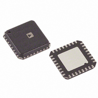
ADN8831ACPZ-R2 Analog Devices Inc, ADN8831ACPZ-R2 Datasheet - Page 15

ADN8831ACPZ-R2
Manufacturer Part Number
ADN8831ACPZ-R2
Description
IC THERMO COOLER CTRLR 32-LFCSP
Manufacturer
Analog Devices Inc
Datasheet
1.ADN8831ACPZ-REEL7.pdf
(20 pages)
Specifications of ADN8831ACPZ-R2
Applications
Thermoelectric Cooler
Current - Supply
8mA
Voltage - Supply
3 V ~ 5.5 V
Operating Temperature
-40°C ~ 85°C
Mounting Type
Surface Mount
Package / Case
32-LFCSP
Laser Driver Type
Thermoelectric Cooler
Supply Current
8mA
Supply Voltage Range
3V To 5.5V
Driver Case Style
LFCSP
No. Of Pins
32
Msl
MSL 1 - Unlimited
Supply Current Max
15mA
Device Type
Laser Diode
Rohs Compliant
Yes
Lead Free Status / RoHS Status
Lead free / RoHS Compliant
The V
values shown in Figure 17, an averaged temperature-to-voltage
coefficient is −25mV/°C at a range of +5°C to +45°C.
PID COMPENSATION AMPLIFIER (CHOP2)
Use the Chop2 amplifier as the PID compensation amplifier.
The voltage at OUT1 feeds into the PID compensation
amplifier. The frequency response of the PID compensation
amplifier is dictated by the compensation network. Apply the
temperature set voltage at IN2P. In Figure 17, the voltage at
OUT2 is expressed as
The user sets the exact compensation network. This network
can vary from a simple integrator to PI, PID, or any other type
of network. The user also determines the type of compensation
and component values because they are dependent on the
thermal response of the object and the TEC. One method for
empirically determining these values is to input a step function
to IN2P, thus changing the target temperature, and adjusting the
compensation network to minimize the settling time of the
object’s temperature.
A typical compensation network used for temperature control
of a laser module is a PID loop consisting of a very low
frequency pole and two separate zeros at higher frequencies.
Figure 19 shows a simple network for implementing PID
compensation. To reduce the noise sensitivity of the control
loop, an additional pole is added at a higher frequency than the
zeros. The bode plot of the magnitude is shown in Figure 20.
The unity-gain crossover frequency of the feed-forward
amplifier is
To ensure stability, the unity-gain crossover frequency should
be lower than the thermal time constant of the TEC and
thermistor. However, this thermal time constant is sometimes
V
f
OUT1
OUT
0
2.5
2.0
1.5
1.0
0.5
dB
0
–15
is centered around V
2
=
=
2
V
π
TEMPSET
R3C1
1
Figure 18. V
5
×
80
−
Z
TEMPERATURE(°C)
Z
×
2
1
OUT1
TECGAIN
(
V
REF
vs. Temperature
OUT
25
/2 at 25°C. With the typical
1
−
V
TEMPSET
45
)
65
Rev. 0 | Page 15 of 20
unspecified making it difficult to characterize. There are many
texts written on loop stabilization, and it is beyond the scope of
this data sheet to discuss all methods and trade offs in
optimizing compensation networks.
MOSFET DRIVER AMPLIFIER
The ADN8831 has two separate MOSFET drivers: a switched
output or pulse-width modulated (PWM) amplifier, and a high
gain linear amplifier. Each amplifier has a pair of outputs that
drive the gates of external MOSFETs which, in turn, drive the
TEC as in Figure 17. A voltage across the TEC is monitored via
SFB and LFB. Although both MOSFET drivers achieve the same
result, to provide constant voltage and high current, their operation
is different. The exact equations for the two outputs are
Where V
V
DD
as
V
V
V
V
V
R2 || R3
B
LFB
SFB
B
B
ADN8831
R1
0dB
=
=
=
R1
R3
OUT2
1
Figure 19. Implementing a PID Compensation Loop
2
2
4
=
=
[ 5 .
0 .
5 .
OUT1
V
V
is the voltage at OUT2 pin. V
3 [
4 [
OUT
Figure 20. Bode Plot for PID Compensation
V
2πR3C1
B
5 .
DD
5 .
R2
−
1
<
2
<
40
<
R3
V
+
V
5
(
V
DD
DD
. 3
( 5
C2
IN2P
OUT
V
] 5
FREQUENCY (Hz LOG SCALE)
]
2πR1C1
2πR1C1
<
OUT
2
. 4
1
1
−
] 5
2
6
. 1
−
IN2N
) 5
. 1
) 5
R1
2πC2 (R2 + R3)
+
CHOP2
CF
–
1
B
C1
is determined by
ADN8831
7
2πR3C2
OUT2
1


