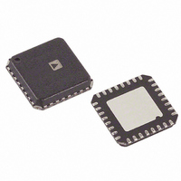
ADN8831ACPZ-R2 Analog Devices Inc, ADN8831ACPZ-R2 Datasheet - Page 6

ADN8831ACPZ-R2
Manufacturer Part Number
ADN8831ACPZ-R2
Description
IC THERMO COOLER CTRLR 32-LFCSP
Manufacturer
Analog Devices Inc
Datasheet
1.ADN8831ACPZ-REEL7.pdf
(20 pages)
Specifications of ADN8831ACPZ-R2
Applications
Thermoelectric Cooler
Current - Supply
8mA
Voltage - Supply
3 V ~ 5.5 V
Operating Temperature
-40°C ~ 85°C
Mounting Type
Surface Mount
Package / Case
32-LFCSP
Laser Driver Type
Thermoelectric Cooler
Supply Current
8mA
Supply Voltage Range
3V To 5.5V
Driver Case Style
LFCSP
No. Of Pins
32
Msl
MSL 1 - Unlimited
Supply Current Max
15mA
Device Type
Laser Diode
Rohs Compliant
Yes
Lead Free Status / RoHS Status
Lead free / RoHS Compliant
ADN8831
PIN CONFIGURATION AND FUNCTION DESCRIPTIONS
Table 4. Pin Function Descriptions
Pin
No.
1
2
3
4
5
6
7
8
9
10
11
12
13
14
15
16
17
18
19
20
21
22
23
24
25
26
27
28
Mnemonic
ILIMC
IN1P
IN1M
OUT1
IN2P
IN2M
OUT2
VREF
AVDD
PHASE
TMPGD
AGND
FREQ
SS/ SB
SYNCO
SYNCI/ SD
COMPOSC
PVDD
SPGATE
SW
SNGATE
PGND
SFB
COMPSW
LPGATE
LNGATE
LFB
CS
Type
Analog Input
Analog Input
Analog Input
Analog Output
Analog Input
Analog Input
Analog Output
Analog Output
Power
Analog Input
Digital Output
Ground
Analog Input
Analog Input
Digital Output
Digital Input
Analog Output
Power
Analog Output
Analog Input
Analog Output
Ground
Analog Input
Analog Input
Analog Output
Analog Output
Analog Input
Analog Input
Description
Sets TEC Cooling Current Limit.
Noninverting Input to Error Amplifier.
Inverting Input to Error Amplifier.
Output of Error Amplifier.
Noninverting Input to Compensation Amplifier.
Inverting Input to Compensation Amplifier.
Output of Compensation Amplifier.
2.5 V Voltage Reference Output.
Power for Nondriver Sections. 3.0 V minimum; 5.5 V maximum.
Sets SYNCO Clock Phase Relative to SYNCI/SD Clock.
Logic Output. Active high. Indicates when OUT1 voltage is within ±100 mV of IN2P voltage.
Analog Ground. Connect to low noise ground.
Sets Switching Frequency with an External Resistor.
Sets Soft Start Time for Output Voltage. Pull low (VTEC = 0 V) to put ADN8831 into standby mode.
Phase Adjustment Clock Output. Phase set from PHASE pin. Used to drive SYNCI/SD of other
ADN8831 devices.
Optional Clock Input. If not connected, clock frequency is set by FREQ pin. Pull low to put
ADN8831 into shutdown mode. Pull high to negate shutdown mode.
Compensation for Oscillator. Connect to PVDD when in free-run mode, connect to R-C
network when in external clock mode.
Power for Output Driver Sections. 3.0 V minimum; 5.5 V maximum.
PWM Output Drives External PMOS Gate.
Connects to PWM FET Drains.
PWM Output Drives External NMOS Gate.
Power Ground. External NMOS devices connect to PGND. Connect to digital ground.
PWM Feedback. Connect to the negative (−) TEC pin of TEC.
Compensation for Switching Amplifier.
Linear Output Drives External PMOS Gate.
Linear Output Drives External NMOS Gate.
Linear Feedback. Connect to the positive (+) TEC pin of TEC.
Connect to Output Current Sense Resistor.
ILIMC
OUT1
OUT2
VREF
IN1M
IN2M
IN1P
IN2P
1
2
3
4
5
6
7
8
Figure 2. Pin Configuration
(Not to Scale)
ADN8831
Rev. 0 | Page 6 of 20
PIN 1
INDICATOR
TOP VIEW
24 COMPSW
23 SFB
22 PGND
21 SNGATE
20 SW
19 SPGATE
18 PVDD
17 COMPOSC


