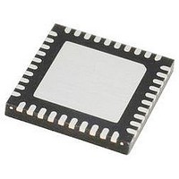
IR3523MTRPBF International Rectifier, IR3523MTRPBF Datasheet - Page 6

IR3523MTRPBF
Manufacturer Part Number
IR3523MTRPBF
Description
IC XPHASE3 CTLR VR11.1 40-MLPQ
Manufacturer
International Rectifier
Series
XPhase3™r
Datasheet
1.IR3523MTRPBF.pdf
(37 pages)
Specifications of IR3523MTRPBF
Applications
Processor
Current - Supply
10mA
Voltage - Supply
4.75 V ~ 7.5 V
Operating Temperature
0°C ~ 100°C
Mounting Type
Surface Mount
Package / Case
40-MLPQ
Ic Function
Dual Output Control IC
Supply Voltage Range
4.75V To 7.5V
Operating Temperature Range
0°C To +150°C
Digital Ic Case Style
MLPQ
No. Of Pins
40
Controller Type
XPhase
Rohs Compliant
Yes
Package
40-Lead MLPQ
Circuit
X-Phase Control IC
Switch Freq (khz)
250kHz to 1.5MHz
Pbf
PbF Option Available
Lead Free Status / RoHS Status
Lead free / RoHS Compliant
Threshold Increasing
Threshold Decreasing
Threshold Hysteresis
Bias Current
Under Voltage Threshold - Voutx
Decreasing
Under Voltage Threshold - Voutx
Increasing
Under Voltage Threshold
Hysteresis
Output Voltage
Leakage Current
VCCL_DRV Activation Threshold
Soft Start and Delay
Start Delay
Start-up Time
OC Delay Time
SS/DELx to FB Input Offset
Voltage
Charge Current
OC Delay Discharge Currents
Fault Discharge Current
Hiccup Duty Cycle
Charge Voltage (Output 1,2)
Delay Comparator Threshold
Delay Comparator Threshold
Delay Comparator Hysteresis
VID1 Sample Delay Comparator
Threshold
Discharge Comp. Threshold
Error Amplifiers
Input Offset Voltage
FB1 Bias Current
FB2 Bias Current
DC Gain
Bandwidth
Slew Rate
Sink Current
Source Current
Maximum Voltage
Minimum Voltage
Open Control Loop Detection
Threshold
Open Control Loop Detection
Delay
ENABLE Inputs
Blanking Time
PGx Outputs
Page 6 of 37
PARAMETER
0V ≤ V(x) ≤ 3.5V
Reference to VDAC
Reference to VDAC
I(PGx) = 4mA
V(PGx) = 5.5V
I(PGx) = 4mA, V(PGx) < 400mV,
V(VCCL) = 0
Measure Enable to EAOUTx activation
Measure Enable activation to PGx
V(IINx) – V(OCSETx) = 500 mV
With FB = 0V, adjust V(SS/DEL) until
EAOUTx drives high
Measure at charge voltage
I(Fault) / I(Charge)
Relative to Charge Voltage, SS/DELx
rising - Note 1
Relative to Charge Voltage, SS/DELx
falling - Note 1
Measure V(FBx) – V(VDACx)). Note 2
Note 1
Note 1
Note 1
Measure V(VCCL) – V(EAOUTx)
Measure V(VCCL) - V(EAOUT), Relative
to Error Amplifier maximum voltage.
Measure PHSOUT pulse numbers from
V(EAOUTx) = V(VCCL) to PGx = low.
Noise Pulse < 100ns will not register an
ENABLE state change. Note 1
25
o
C ≤ T
J
TEST CONDITION
≤ 100
o
C
MIN
1.38
-365
-325
-5%
470
200
150
100
500
125
0.8
1.0
0.7
-30
2.5
3.5
2.8
5.5
0.4
5.0
20
75
-5
-1
-1
5
1
3
8
Vrosc(V)*100
0 /Rosc(K )
TYP
1.65
0.99
-315
-275
0.85
620
150
650
135
200
110
780
120
300
250
-50
2.0
2.9
1.4
4.5
3.9
3.0
8.5
53
47
10
70
65
30
12
0
0
June 20, 2008
8
0
0
8
IR3523
MAX
1000
1.94
-265
-225
+5%
12.0
300
135
950
250
600
800
400
110
300
3.5
1.9
-70
6.5
4.2
3.2
1.2
3.6
13
12
40
20
10
1
1
1
5
µA/µA
UNIT
Pulse
MHz
V/µs
mV
mV
mV
mV
mV
mA
mA
mV
mV
mV
mV
mV
mV
mV
mV
ms
ms
µA
µA
µA
µA
µA
dB
uA
µA
us
ns
V
V
V
V
V
V


