L9951 STMicroelectronics, L9951 Datasheet - Page 23
L9951
Manufacturer Part Number
L9951
Description
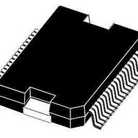
IC REAR DOOR ACT DVR POWERSO-36
Manufacturer
STMicroelectronics
Type
DC Motor Driverr
Datasheet
1.L9951XPTR.pdf
(36 pages)
Specifications of L9951
Applications
Automotive
Current - Supply
7mA
Voltage - Supply
7 V ~ 28 V
Operating Temperature
-40°C ~ 150°C
Mounting Type
Surface Mount
Package / Case
PowerSO-36 Exposed Bottom Pad
Operating Current
20mA
Operating Temperature Classification
Automotive
Motor Controller Type
DC Motor Driver
Package Type
PowerSO
Operating Supply Voltage (min)
7V
Operating Supply Voltage (max)
28V
Supply Current
20 mA
Mounting Style
SMD/SMT
Lead Free Status / RoHS Status
Lead free / RoHS Compliant
Available stocks
Company
Part Number
Manufacturer
Quantity
Price

Part Number:
L9951
Manufacturer:
ST
Quantity:
20 000
Part Number:
L9951XP
Manufacturer:
ST
Quantity:
20 000
Company:
Part Number:
L9951XPTR
Manufacturer:
st
Quantity:
6 966
Part Number:
L9951XPTR
Manufacturer:
ST
Quantity:
20 000


L9951 / L9951XP
4.4
4.5
4.6
4.7
4.8
Serial Data Out (DO)
The data output driver is activated by a logical low level at the CSN input and will go from
high impedance to a low or high level depending on the status bit 0 (fault condition). The first
rising edge of the CLK input after a high to low transition of the CSN pin will transfer the
content of the selected status register into the data out shift register. Each subsequent
falling edge of the CLK will shift the next bit out.
Serial clock (CLK)
The CLK input is used to synchronize the input and output serial bit streams. The data input
(DI) is sampled at the rising edge of the CLK and the data output (DO) will change with the
falling edge of the CLK signal.
Input data register
The device has two input registers. The first bit (bit 0) at the DI-input is used to select one of
the two input registers. All bits are first shifted into an input shift register. After the rising
edge of CSN the contents of the input shift register will be written to the selected input data
register only if a frame of exact 16 data bits are detected. Depending on bit 0 the contents of
the selected status register will be transferred to DO during the current communication
frame. Bit 1-8 control the behavior of the corresponding driver. The bits 9,10 and 11 are
used to control the current monitor multiplexer. Bit 15 is used to reset all status bits in both
status registers. The bits in the status registers will be cleared after the current
communication frame (rising edge of CSN).
Status register
This devices uses two status registers to store and to monitor the state of the device. Bit 0 is
used as a fault bit and is a logical-NOR combination of bits 1-14 in both status registers. The
state of this bit can be polled by the microcontroller without the need of a full SPI-
communication cycle (see
driver will be disabled. If the over-current recovery bit of the output is not set the
microcontroller has to clear the over-current bit to enable the driver. If the thermal shutdown
bit is set, all drivers will go into a high impedance state. Again the microcontroller has to
clear the bit to enable the drivers.
Test mode
The test mode can be entered by rising the CSN input to a voltage higher than 7.5V. In the
test mode the inputs CLK, DI, PWM and the internal 2MHz CLK can be multiplexed to data
output DO for testing purpose. Furthermore the over-current thresholds are reduced by a
factor of 4 to allow EWS testing at lower current. The internal logic prevents that the Hi-Side
and Low-Side driver of the same half-bridge can be switched-on at the same time. In the test
mode this combination is used to multiplex the desired signals to the CM output according to
table 18 and 19.
Figure
Doc ID 14173 Rev 8
8.). If one of the over-current bits is set, the corresponding
Functional description of the SPI
23/36
Related parts for L9951
Image
Part Number
Description
Manufacturer
Datasheet
Request
R

Part Number:
Description:
STMicroelectronics [RIPPLE-CARRY BINARY COUNTER/DIVIDERS]
Manufacturer:
STMicroelectronics
Datasheet:
Part Number:
Description:
STMicroelectronics [LIQUID-CRYSTAL DISPLAY DRIVERS]
Manufacturer:
STMicroelectronics
Datasheet:

Part Number:
Description:
BOARD EVAL FOR MEMS SENSORS
Manufacturer:
STMicroelectronics
Datasheet:
Part Number:
Description:
NPN TRANSISTOR POWER MODULE
Manufacturer:
STMicroelectronics
Datasheet:
Part Number:
Description:
TURBOSWITCH ULTRA-FAST HIGH VOLTAGE DIODE
Manufacturer:
STMicroelectronics
Datasheet:
Part Number:
Description:
Manufacturer:
STMicroelectronics
Datasheet:
Part Number:
Description:
DIODE / SCR MODULE
Manufacturer:
STMicroelectronics
Datasheet:
Part Number:
Description:
DIODE / SCR MODULE
Manufacturer:
STMicroelectronics
Datasheet:
Part Number:
Description:
Search -----> STE16N100
Manufacturer:
STMicroelectronics
Datasheet:
Part Number:
Description:
Search ---> STE53NA50
Manufacturer:
STMicroelectronics
Datasheet:
Part Number:
Description:
NPN Transistor Power Module
Manufacturer:
STMicroelectronics
Datasheet:
Part Number:
Description:
DIODE / SCR MODULE
Manufacturer:
STMicroelectronics
Datasheet: