L9949 STMicroelectronics, L9949 Datasheet - Page 4
L9949
Manufacturer Part Number
L9949
Description
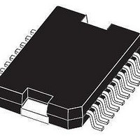
IC DRIVER DOOR ACTUATOR PWRSO-20
Manufacturer
STMicroelectronics
Type
Door Actuator Driverr
Datasheet
1.L9949TR.pdf
(20 pages)
Specifications of L9949
Applications
Automotive
Current - Supply
7mA
Voltage - Supply
7 V ~ 28 V
Operating Temperature
-40°C ~ 150°C
Mounting Type
Surface Mount
Package / Case
PowerSO-20 Exposed Bottom Pad
Product
Half-Bridge Drivers
Supply Current
20 mA
Mounting Style
SMD/SMT
Lead Free Status / RoHS Status
Lead free / RoHS Compliant
Available stocks
Company
Part Number
Manufacturer
Quantity
Price

Part Number:
L9949TR
Manufacturer:
ST
Quantity:
20 000


L9949
PIN FUNCTION
4/20
5, 8, 13,
11, 20
1, 10,
N°
18
15
14
17
16
12
19
6
7
9
2
3
4
Data Out Serial data output:
Data In
OUT1
OUT2
OUT3
OUT4
OUT5
OUT6
GND
CSN
CLK
V
Pin
CM
V
CC
S
Ground:
Reference potential
Important: For the capability of driving the full current at the outputs all pins of GND must be
externally connected !
Power supply voltage (battery):
For this input a ceramic capacitor as close as possible to GND is recommended.
Important: For the capability of driving the full current at the outputs all pins of V
externally connected !
Logic supply voltage:
For this input a ceramic capacitors as close as possible to GND are recommended.
Chip Select Not input:
This input is low active and requires CMOS logic levels. The serial data transfer between L9949
and micro controller is enabled by pulling the input CSN to low level. If an input voltage of more
than 9.6V above VCC is applied to CSN pin the L9949 will be switched into a test mode.
Serial clock input:
This input controls the internal shift register of the SPI and requires CMOS logic levels.
Serial data input:
The input requires CMOS logic levels and receives serial data from the microcontroller. The data
is an 16bit control word and the least significant bit (LSB, bit 0) is transferred first.
The diagnosis data is available via the SPI and this tristate-output. The output will remain in
tristate, if the chip is not selected by the input CSN (CSN = high)
Current monitor output:
Depending on the multiplexer bits 12 and 13 of the Input Data register this output sources an
image of the instant current through the corresponding highside driver with a ratio of 1/10000
Halfbridge-output 1:
The output is built by a highside and a lowside switch, which are internally connected. The
output stage of both switches is a power DMOS transistor. Each driver has an internal parasitic
reverse diode (bulk-drain-diode, highside driver from OUT1 to V
OUT1). This output is overcurrent and open load protected.
Halfbridge-output 2:
Halfbridge-output 3:
The output is built by a highside and a lowside switch, which are internally connected. The
output stage of both switches is a power DMOS transistor. Each driver has an internal parasitic
reverse diode (bulk-drain-diode, highside driver from OUT3 to VS, lowside driver from GND to
OUT3). This output is overcurrent and open load protected.
Halfbridge-output 4:
Halfbridge-output 5:
Highside-driver-output 6:
The output is built by a highside switch and can be used only for a resistive load, because the
internal reverse diode from GND to OUT6 is missing. This highside switch is a power DMOS
transistor with an internal parasitic reverse diode from OUT6 to V
is overcurrent and open load protected.
see OUT1 (pin 9)
see OUT3 (pin 2)
see OUT3 (pin 2)
Description
S
S
, lowside driver from GND to
(bulk-drain-diode). The output
S
must be
Related parts for L9949
Image
Part Number
Description
Manufacturer
Datasheet
Request
R

Part Number:
Description:
STMicroelectronics [RIPPLE-CARRY BINARY COUNTER/DIVIDERS]
Manufacturer:
STMicroelectronics
Datasheet:
Part Number:
Description:
STMicroelectronics [LIQUID-CRYSTAL DISPLAY DRIVERS]
Manufacturer:
STMicroelectronics
Datasheet:

Part Number:
Description:
BOARD EVAL FOR MEMS SENSORS
Manufacturer:
STMicroelectronics
Datasheet:
Part Number:
Description:
NPN TRANSISTOR POWER MODULE
Manufacturer:
STMicroelectronics
Datasheet:
Part Number:
Description:
TURBOSWITCH ULTRA-FAST HIGH VOLTAGE DIODE
Manufacturer:
STMicroelectronics
Datasheet:
Part Number:
Description:
Manufacturer:
STMicroelectronics
Datasheet:
Part Number:
Description:
DIODE / SCR MODULE
Manufacturer:
STMicroelectronics
Datasheet:
Part Number:
Description:
DIODE / SCR MODULE
Manufacturer:
STMicroelectronics
Datasheet:
Part Number:
Description:
Search -----> STE16N100
Manufacturer:
STMicroelectronics
Datasheet:
Part Number:
Description:
Search ---> STE53NA50
Manufacturer:
STMicroelectronics
Datasheet:
Part Number:
Description:
NPN Transistor Power Module
Manufacturer:
STMicroelectronics
Datasheet:
Part Number:
Description:
DIODE / SCR MODULE
Manufacturer:
STMicroelectronics
Datasheet: