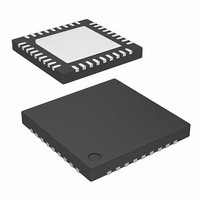
ISL97651ARTZ-TK Intersil, ISL97651ARTZ-TK Datasheet - Page 14

ISL97651ARTZ-TK
Manufacturer Part Number
ISL97651ARTZ-TK
Description
IC LCD SUPPLY HP 4CHN 36-TQFN
Manufacturer
Intersil
Datasheet
1.ISL97651ARTZ-TK.pdf
(19 pages)
Specifications of ISL97651ARTZ-TK
Applications
LCD TV/Monitor
Current - Supply
400µA
Voltage - Supply
4 V ~ 5.5 V
Operating Temperature
-40°C ~ 105°C
Mounting Type
Surface Mount
Package / Case
36-TQFN
Lead Free Status / RoHS Status
Lead free / RoHS Compliant
Output Capacitor (Buck Converter)
Four 10µF or two 22µF ceramic capacitors are
recommended for this part. The overshoot and undershoot
will be reduced with more capacitance, but the recovery time
will be longer.
PI Loop Compensation (Buck Converter)
The buck converter of ISL97651 can be compensated by a
RC network connected from CM2 pin to ground. C9 = 4.7nF
and R2 = 2k RC network is used in the demo board. The
larger value resistor can lower the transient overshoot,
however, at the expense of stability of the loop.
The stability can be optimized in a similar manner to that
described in “PI Loop Compensation (Boost Converter)” on
page 12.
Bootstrap Capacitor (C16)
This capacitor is used to provide the supply to the high driver
circuitry for the buck MOSFET. The bootstrap supply is
formed by an internal diode and capacitor combination. A
1µF is recommended for ISL97651. A low value capacitor
can lead to overcharging and in turn damage the part.
If the load is too light, the on-time of the low side diode may
be insufficient to replenish the bootstrap capacitor voltage. In
this case, if V
up device may be unable to turn-on until V
Hence, there is a minimum load requirement in this case.
The minimum load can be adjusted by the feedback
resistors to FBL.
The bootstrap capacitor can only be charged when the
higher side MOSFET is off. If the load is too light which can
not make the on time of the low side diode be sufficient to
replenish the boot strap capacitor, the MOSFET can’t turn
on. Hence there is minimum load requirement to charge the
bootstrap capacitor properly.
Linear-Regulator Controllers (V
The ISL97651 include 2 independent charge pumps (see
Figure 13). The negative charge pump inverters the V
voltage and provides a regulated negative output voltage.
The positive charge pump doubles or triples the V
voltage and provides a regulated positive output voltage.
The regulation of both the negative and positive charge
pumps is generated by internal comparator that senses the
output voltage and compares it with the internal reference.
TABLE 9. BUCK OUTPUT CAPACITOR RECOMMENDATION
CAPACITOR
100µF/6.3V
10µF/6.3V
10µF/6.3V
22µF/6.3V
IN
- V
SIZE
0805 TDK
0805 Murata
1210 TDK
1206 Murata
BUCK
< 1.5V, the internal MOSFET pull-
VENDOR
14
C2012X5R0J106M
GRM21BR60J106K
C3216X5R0J226M
GRM31CR60J107M
ON
PART NUMBER
and V
LOGIC
OFF
falls.
SUP
)
SUP
ISL97651
The pumps use pulse width modulation to adjust the pump
period, depending on the load present. The pumps can
provide 30mA for V
The positive charge pump can generate double or triple
V
C2- pins. If the C2+ pin connects to C1+, it is the voltage
doubler, and if C2+ connects C2- via a capacitor, it
configured a voltage tripler.
Positive Charge Pump Design Consideration
The positive charge pump integrates all the diodes (D1, D2
and D3 shown in the block diagram in Figure 13) required for
x2 (V
During the chip start-up sequence the mode of operation is
automatically detected when the charge pump is enabled.
With both C7 and C8 present, the x3 mode of operation is
detected. With C7 present, C8 open and with C1+ shorted to
C2+, the x2 mode of operation will be detected.
Due to the internal switches to V
P
pump is enabled. This is important for TFT applications
where the negative charge pump output voltage (V
A
The maximum P
from Equation 15 assuming a 50% switching duty:
Note: V
function of I
In voltage doubler configuration, the maximum V
given by Equation 16:
For Voltage Tripler:
V
V
I
2 V
---------------------------------------------------------------------------------------------------------------------- 0.95A
I
V
3 V
---------------------------------------------------------------------------------------------------------------------- 0.95V
MAX
V
MAX
VDD
SUP
OUT
ON_MAX(3x)
ON
ON
•
•
ON_MAX(2x)
SUP
SUP
(
(
SUP
output voltage is determined by Equation 18:
=
2x
3x
supplies need to be established before P
voltage depending on the configuration of C2+ and
is independent of the voltage on V
(
DIODE
V
)
)
2
(
FBP
–
–
∼
∼
2
doubler) and x3 (V
•
2
3
min of 50mA or
min of 50mA or
•
(
MAX
3 R
•
•
(
=
•
2 R
V
V
•
=
(2 • I
⎛
⎜
⎝
DIODE
•
DIODE
3
1
2
OUT
ONH
and V
•
+
•
ONH
(
R
------ -
R
(
V
OFF
MAX
V
8
9
SUP
charge pump current can be estimated
SUP
⎞
⎟
⎠
(
(
+
2 I
2 I
DIODE
+
2 R
) is the on-chip diode voltage as a
•
and 20mA for V
•
R
•
–
–
MAX
ONL
MAX
V
V
ONL
DIODE
SUP
DIODE
(40mA) < 0.7V.
) V V
)
) V V
)
–
–
)
SUP
)
tripler) modes of operation.
)
(
(
)
–
–
ON
ON
2 I
(M1, M2 and M3),
2 I
•
•
)
)
ON
SUP
OUT
•
•
OUT
.
until the charge
•
•
(
OUT
(
3 r
2 r
ON
•
•
OFF
April 24, 2009
ONH
.
ONH
is as
(EQ. 17)
(EQ. 16)
(EQ. 15)
(EQ. 18)
FN7493.3
) and
+
+
2 r
r
ONL
•
ONL
)
)


