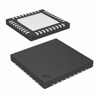
ISL97651ARTZ-TK Intersil, ISL97651ARTZ-TK Datasheet - Page 16

ISL97651ARTZ-TK
Manufacturer Part Number
ISL97651ARTZ-TK
Description
IC LCD SUPPLY HP 4CHN 36-TQFN
Manufacturer
Intersil
Datasheet
1.ISL97651ARTZ-TK.pdf
(19 pages)
Specifications of ISL97651ARTZ-TK
Applications
LCD TV/Monitor
Current - Supply
400µA
Voltage - Supply
4 V ~ 5.5 V
Operating Temperature
-40°C ~ 105°C
Mounting Type
Surface Mount
Package / Case
36-TQFN
Lead Free Status / RoHS Status
Lead free / RoHS Compliant
V
The V
switching the voltage on COM between ground, DRN and SRC,
under control of the start-up sequence and the CTL pin.
During the start-up sequence, COM is held at ground via an
NDMOS FET, with ~1k impedance. Once the start-up
sequence has completed, CTL is enabled and acts as a
multiplexer control such that if CTL is low, COM connects to
DRN through a 30Ω internal MOSFET, and if CTL is high,
COM connects to P
The slew rate of start-up of the switch control circuit is mainly
restricted by the load capacitance at COM pin as
Equation 21:
RWhere V
at P
between COM and DRN or P
MOSFET r
inserted, R
and C
In the “Typical Application Diagram” on page 10, R10, R11
and C15 give the bias to DRN based on Equation 22:
And R12 can be adjusted to adjust the slew rate.
ΔV
------- -
V
Δt
DRN
ON
=
OUT
Slice Circuit
ON
------------------------------------ -
(
L
=
R
is the load capacitance of switch control circuit.
, which range is from 0V to 36V. R
i
V
-------------------------------------------------------------- -
Slice Circuit functions as a three way multiplexer,
||
ON
g
R
DS(On)
L
V
L
is the supply voltage applied to DRN or voltage
g
is the load resistance of switch control circuit,
) C
⋅
FAULT
×
R
R
11
10
L
, the trace resistance and the resistor
+AVDD R
+
1.2MHz
OUT
R
11
A2
CLK
EN
internally via a 5Ω MOSFET.
⋅
10
16
OUT
0.4V
STOP
CONTROL
including the internal
PWM
A1
FIGURE 14. NEGATIVE CHARGE PUMP BLOCK DIAGRAM
VDD
i
is the resistance
0.2V
(EQ. 21)
(EQ. 22)
M2
M1
ISL97651
VSUP
PGND
NOUT
FBN
820pF
Start-Up Sequence
Figure 15 shows a detailed start up sequence waveform. For
a successful power up, there should be 6 peaks at V
When a fault is detected, the device will latch off until either
EN is toggled or the input supply is recycled.
When the input is higher than 2.75V; if either EN or ENL is H,
V
internal current source starts to charge C
threshold using a fast ramp followed by a slow ramp. Several
more ramps follow, during which time the device checks for
fault conditions. If a fault is found, the sequence is halted.
Initially the boost is not enabled so A
V
at A
not desirable, an external PMOS FET can be used to delay
the output until the boost is enabled internally. The delayed
output appears at A
A
start ramp depends on the value of the C
range of C
C
V
DELB gate goes low to turn on the external PMOS to
generate a delayed A
V
Once the start-up sequence is complete, the voltage on the
C
or the EN pin is disabled. If a fault is detected, the voltage on
C
power is cycled or enable is toggled.
VDD
REF
IN
OFF
ON
DLY
DLY
DLY
C20
VDD
- V
220nF
is enabled at the beginning of the sixth ramp.
C12
capacitor remains at 1.15V until either a fault is detected
of 220nF, the soft-start time is ~8ms.
rises to 2.4V at which point the chip is disabled until the
turns on. If ENL is H, V
turns on at the start of the fourth peak, at the same time
soft-starts at the beginning of the third ramp. The soft-
DIODE
V
REF
during this part of the start up sequence. If this step is
DLY
R6
40k
through the output diode. Hence, there is a step
capacitor value is from 10nF to 220nF. For
D3
VDD
VDD
100pF
328k
C19
R7
D2
.
output.
LOGIC
turns on. If EN is H, an
VDD
C13
470nF
V
OFF
CDLY
DLY
rises to
(-8V)
capacitor. The
to an upper
April 24, 2009
CDLY
FN7493.3
.


