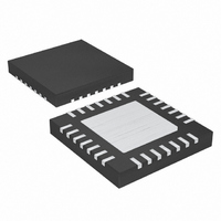
MAX8819CETI+ Maxim Integrated Products, MAX8819CETI+ Datasheet - Page 14

MAX8819CETI+
Manufacturer Part Number
MAX8819CETI+
Description
IC PMIC W/INT CHARGER 28TQFN-EP
Manufacturer
Maxim Integrated Products
Type
PMIC with Integrated Chargersr
Datasheet
1.MAX8819CETIT.pdf
(29 pages)
Specifications of MAX8819CETI+
Applications
Handheld/Mobile Devices
Voltage - Supply
4.1 V ~ 5.5 V
Operating Temperature
-40°C ~ 85°C
Mounting Type
Surface Mount
Package / Case
28-TQFN Exposed Pad
Output Voltage Range
1 V to 4 V
Input Voltage Range
4.1 V to 5.5 V
Input Current
1.33 mA
Power Dissipation
2285.7 mW
Operating Temperature Range
- 40 C to + 85 C
Mounting Style
SMD/SMT
Lead Free Status / RoHS Status
Lead free / RoHS Compliant
Current - Supply
-
Lead Free Status / Rohs Status
Lead free / RoHS Compliant
PMIC with Integrated Chargers and Smart
Power Selector in a 4mm x 4mm TQFN
14
______________________________________________________________________________________
PIN
14
15
16
17
18
19
20
21
22
23
24
25
26
27
28
—
NAME
DLIM1
EN123
DLIM2
CISET
PV13
CHG
PG1
PG3
PG2
FB2
FB3
LX1
LX3
PV2
LX2
EP
Charge Rate Select Input. Connect a resistor from CISET to GND (R
current limit, prequalification-charge current limit, and top-off threshold.
Active-Low, Open-Drain Charge Status Output. CHG pulls low to indicate that the battery is charging.
See Figure 3 for more information.
REG1 Power Ground
Inductor Switching Node for REG1. When enabled, LX1 switches between PV13 and PG1 to regulate
the FB1 voltage to 1.0V. When disabled, LX1 is pulled to PG1 by 1kΩ in shutdown.
Power Input for the REG1 and REG3 Converters. Connect PV13 to SYS. Bypass PV13 to PG1 with a
4.7μF ceramic capacitor.
Inductor Switching Node for REG3. When enabled, LX3 switches between PV13 and PG3 to regulate
the FB3 voltage to 1.0V. When disabled, LX3 is pulled to PG3 by a 1kΩ internal resistor.
REG3 Power Ground
Input Current-Limit Selection Digital Input 1. Drive high or low according to Table 1 to set the DC input
current limit.
Feedback Input for REG2. Connect FB2 to the center of a resistor voltage-divider from the REG2
output capacitors to GND to set the output voltage from 1V to V
REG2 is disabled by grounding PV2.
Feedback Input for REG3. Connect FB3 to the center of a resistor voltage-divider from the REG3
output capacitors to GND to set the output voltage from 1V to V
RE G1, RE G2, and RE G3 E nab l e Inp ut. D r i ve E N 123 hi g h to enab l e RE G1, RE G 2, and RE G3. D r i ve E N 123
l ow to d i sab l e RE G 1, RE G2, and RE G 3. The enab l e/d i sab l e seq uenci ng i s show n i n Fi g ur es 6 and 7.
Power Input for REG2. Connect PV2 to SYS for normal operation. Bypass PV2 to PG2 with a 2.2μF
ceramic capacitor. For systems that do not require REG2, connect PV2, FB2, and PG2 to GND (LX2
may be unconnected or connected to GND).
Inductor Switching Node for REG2. When enabled, LX2 switches between PV2 and PG2 to regulate
the FB2 voltage to 1.0V. When disabled, LX2 is pulled to PG2 by a 1kΩ internal resistor.
REG2 Power Ground
Input Current-Limit Selection Digital Input 2. Drive high or low according to Table 1 to set the DC input
current limit.
Exposed Pad
FUNCTION
Pin Description (continued)
SYS
SYS
. FB2 must be connected to GND if
.
CISET
) to set the fast-charge


