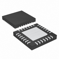
MAX8819CETI+ Maxim Integrated Products, MAX8819CETI+ Datasheet - Page 28

MAX8819CETI+
Manufacturer Part Number
MAX8819CETI+
Description
IC PMIC W/INT CHARGER 28TQFN-EP
Manufacturer
Maxim Integrated Products
Type
PMIC with Integrated Chargersr
Datasheet
1.MAX8819CETIT.pdf
(29 pages)
Specifications of MAX8819CETI+
Applications
Handheld/Mobile Devices
Voltage - Supply
4.1 V ~ 5.5 V
Operating Temperature
-40°C ~ 85°C
Mounting Type
Surface Mount
Package / Case
28-TQFN Exposed Pad
Output Voltage Range
1 V to 4 V
Input Voltage Range
4.1 V to 5.5 V
Input Current
1.33 mA
Power Dissipation
2285.7 mW
Operating Temperature Range
- 40 C to + 85 C
Mounting Style
SMD/SMT
Lead Free Status / RoHS Status
Lead free / RoHS Compliant
Current - Supply
-
Lead Free Status / Rohs Status
Lead free / RoHS Compliant
PMIC with Integrated Chargers and Smart
Power Selector in a 4mm x 4mm TQFN
current is first reduced by lowering charge current. If
the junction temperature still reaches +120°C in spite of
charge current reduction, no input current is drawn
from DC; the battery supplies the entire load and SYS is
regulated 70mV below BAT.
The IC disables all regulator outputs and the battery
charger when the junction temperature rises above
+165°C, allowing the device to cool. When the junction
temperature cools by approximately 15°C the regula-
tors and charger resume the state indicated by the
enable input (EN123, EN4, and CEN) by repeating their
soft-start sequence. Please note that this thermal-over-
load shutdown is a fail-safe mechanism; proper thermal
design should ensure that the junction temperature of
the MAX8819_ never exceeds the absolute maximum
rating of +150°C.
Dynamic output voltage adjustment can be implement-
ed for the step-down converter by adding a resistor
and a switch from FB_ to GND. See Figure 9.
To calculate the resistor-divider, start with the lower
voltage desired and calculate the resistor-divider using
R
the following equation to calculate R
where V
V
Figure 9. Dynamic Output Voltage Control
28
FB
T
and R
is the feedback regulation voltage, 1V (typ).
______________________________________________________________________________________
Dynamic Output Voltage Adjustment
OUTL
B
only. Setting R
Regulator Thermal-Overload Shutdown
is the desired lower output voltage and
Applications Information
R
FB_
T
=
R
for Step-Down Converters
R
B
R
B
T
OUT_
×
B
⎛
⎜
⎝
= 100kΩ is acceptable. Use
V
OUTL
V
FB
−
R
T
D
⎟ 1
:
⎞
⎠
R
following equations assuming the switch resistance is
negligible:
where R
V
back regulation voltage, 1V (typ).
For example, if V
100kΩ, then:
Choose R
The scope plot (Figure 10) shows V1 switching from 3V
to 3.3V to 3V with the resistor values of the example.
When the switch is turned on, V1 slews from 3V to 3.3V
in about 20μs, which is less than the 50μs RST1 de-
glitch filter, and therefore, RST1 does not trip. When the
switch is turned off, V1 soars to about 3.35V due to the
energy in the inductor. Since V1 is above the regulation
voltage, REG1 skips until V1 decays to the regulation
voltage. The decay rate is determined by the output
capacitance and the load. In this example, the output
capacitance is 10μF and the load is 10Ω, so the time
Figure 10. Dynamic Voltage Adjustment with Example Values
OUTH
D
is calculated using the higher set voltage and the
CH2 = V1, 1V offset; 3V to 3.3V to 3V, 10Ω load
R
GATE DRIVE
TO SWITCH
D
is the higher set voltage, and V
R
PAR
PAR
= 1/((1/86.96kΩ) - (1/100kΩ)) = 666.7kΩ
D
R
RST1
T
= 665kΩ as the closest standard 1% value.
V1
= 100kΩ x ((3V/1V) - 1) = 200kΩ
is the parallel resistance of R
= 200kΩ/((3.3V/1V) - 1) = 86.96kΩ
CH1 = gate drive to switch
3V
R
R
PAR
D
OUTL
=
3.3V
CH3 = RST1
R
=
PAR
1
V
100μs/div
3.35V
= 3V, V
OUTH
V
1
FB
R
−
T
R
1
B
−
1
OUTH
FB
= 3.3V, R
5V/div
0V
500mV/div
3V
4.2V
2V/div
is the feed-
B
and R
B
D
=
,


