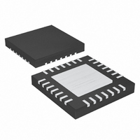
MAX8819CETI+ Maxim Integrated Products, MAX8819CETI+ Datasheet - Page 16

MAX8819CETI+
Manufacturer Part Number
MAX8819CETI+
Description
IC PMIC W/INT CHARGER 28TQFN-EP
Manufacturer
Maxim Integrated Products
Type
PMIC with Integrated Chargersr
Datasheet
1.MAX8819CETIT.pdf
(29 pages)
Specifications of MAX8819CETI+
Applications
Handheld/Mobile Devices
Voltage - Supply
4.1 V ~ 5.5 V
Operating Temperature
-40°C ~ 85°C
Mounting Type
Surface Mount
Package / Case
28-TQFN Exposed Pad
Output Voltage Range
1 V to 4 V
Input Voltage Range
4.1 V to 5.5 V
Input Current
1.33 mA
Power Dissipation
2285.7 mW
Operating Temperature Range
- 40 C to + 85 C
Mounting Style
SMD/SMT
Lead Free Status / RoHS Status
Lead free / RoHS Compliant
Current - Supply
-
Lead Free Status / Rohs Status
Lead free / RoHS Compliant
PMIC with Integrated Chargers and Smart
Power Selector in a 4mm x 4mm TQFN
In addition to charging the battery, the IC supplies
power to the system through the SYS output. The
charging current is provided from SYS so that the set
input current limit controls the total SYS current, this is
the sum of the system load current and the battery-
charging current.
In some instances, there may not be enough DC input
current to supply peak system loads. The Smart Power
Selector circuitry offers flexible power distribution from
an AC-to-DC adapter or USB source to the battery and
system load. The battery is charged with any available
power not used by the system load. If a system load
peak exceeds the input current limit, supplemental cur-
rent is taken from the battery. Thermal limiting prevents
overheating by reducing power drawn from the input
source. In the past, it might have been necessary to
reduce system functionality to limit current drain when a
USB source is connected. However, with the
MAX8819_, this is no longer the case. When the DC or
USB source hits its limit, the battery supplies supple-
mental current to maintain the load.
The IC features overvoltage protection. Part of this protec-
tion is a 4.35V (MAX8819A/MAX8819C) or 5.3V
(MAX8819B) voltage limiter at SYS. If DC exceeds the
overvoltage threshold of 5.88V (V
iter disconnects SYS from DC, but battery-powered oper-
ation of all regulators is still allowed.
The Smart Power Selector seamlessly distributes power
between the current-limited external input (DC), the bat-
tery (BAT), and the system load (SYS). The basic func-
tions performed are:
With both an external power supply (DC) and battery
(BAT) connected:
• When the system load requirements are less than
• When the system load requirements exceed the
• When the battery is connected and there is no exter-
• When an external power input is connected and
16
the input current limit, the battery is charged with
residual power from the input.
input current limit, the battery supplies supplemental
current to the load through the internal system load
switch.
nal power input, the system (SYS) is powered from
the battery.
there is no battery, the system (SYS) is powered
from the external power input.
______________________________________________________________________________________
OVLO_DC
Input Limiter
), the input lim-
A thermal-limiting circuit reduces the battery charge
rate and external power source current to prevent the
MAX8819_ from overheating.
An internal 70mΩ MOSFET connects SYS to BAT when
no voltage source is available at DC. When an external
source is detected at DC, this switch opens and SYS is
powered from the valid input source through the Smart
Power Selector.
When the system load requirements exceed the input
current limit, the battery supplies supplemental current
to the load through the internal system load switch. If
the system load continuously exceeds the input current
limit, the battery does not charge, even though external
power is connected. This is not expected to occur in
most cases because high loads usually occur only in
short peaks. During these peaks, battery energy is
used, but at all other times the battery charges.
DC is a current-limited power input that supplies the
system (SYS) up to 1A. The DC to SYS switch is a linear
regulator designed to operate in dropout. This linear
regulator prevents the SYS voltage from exceeding
5.3V for the MAX8819B or 4.35V for the MAX8819A/
MAX8819C. As shown in Table 1, DC supports four dif-
ferent current limits that are set with the DLIM1 and
DLIM2 digital inputs. These current limits are ideally suit-
ed for use with AC-to-DC wall adapters and USB power.
The operating voltage range for DC is 4.1V to 5.5V, but it
can tolerate up to 6V without damage. When the DC
input voltage is below the undervoltage threshold (4V), it
is considered invalid. When the DC voltage is below the
battery voltage it is considered invalid. The DC power
input is disconnected when the DC voltage is invalid.
Bypass DC to ground with at least a 4.7μF capacitor.
Four current settings are provided based upon the set-
tings of DLIM1 and DLIM2, see Table 1. DLIM1 and
DLIM2 are deglitched. This deglitching prevents the
problem of major carry transitions momentarily entering
the suspend state.
Table 1. DC Current-Limit Settings
DLIM1
0
0
1
1
DLIM2
DC Power Input (DC, DLIM1, DLIM2)
0
1
0
1
System Load Switch
DC I
Suspend
1000
LIM
475
95
(mA)


