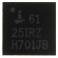
ISL6125IRZA Intersil, ISL6125IRZA Datasheet - Page 18

ISL6125IRZA
Manufacturer Part Number
ISL6125IRZA
Description
IC POWER SUPPLY SEQUENCER 24QFN
Manufacturer
Intersil
Datasheet
1.ISL6123IRZA.pdf
(22 pages)
Specifications of ISL6125IRZA
Applications
Power Supply Sequencer
Voltage - Supply
1.5 V ~ 5.5 V
Current - Supply
200µA
Operating Temperature
-40°C ~ 85°C
Mounting Type
Surface Mount
Package / Case
24-VQFN
Lead Free Status / RoHS Status
Lead free / RoHS Compliant
Voltage - Input
-
If the mere presence of some voltage potential is adequate
prior to sequencing on, then a small number of standard
logic AND gates can be used to accomplish this. The block
diagram in Figure 19 illustrates this voltage presence
configuration.
In either case, the sequencing is straight forward across
multiple sequencers as all DLY_ON capacitors will
simultaneously start charging ~10ms after the common
ENABLE input signal is delivered. This allows the choice of
capacitors to be related to each other no different than using
a single sequencer. When the common enabling signal is
de-asserted these configurations will then execute the
turn-off sequence across all sequencers as programmed by
the DLY_OFF capacitor values.
In both cases, with all the SYSRST pins bussed together,
once the on sequence is complete, simultaneous shutdown
upon any UVLO input failure is assured as SYSRST output
will momentarily pull low turning off all GATE and LOGIC
outputs.
There may be applications that require or allow groups of
supplies being brought up in sequence and supplies within
each group to be sequenced. Figure 20 illustrates such a
configuration that allows the first group of supplies to turn-on
before the second group starts. This arrangement does not
necessarily preclude adding the assurance of all supplies
prior to turn-on sequencing as previously shown but it will
RESET
en
SUPPLY
POWER
FIGURE 18. ISL612X AND ISL613X VOLTAGE COMPLIANT
PGOOD
ON ALL RAILS
MONITORING
ISL6131 or 32
SEQUENCING BLOCK DIAGRAM
VMON
ISL6123, ISL6124, ISL6125, ISL6126, ISL6127, ISL6128, ISL6130
18
UVLO
SYSRST
RESET
RESET
UVLO
SYSRST
ISL6125
ISL6124
# N
ENABLE
ENABLE
# N+1
O
G
C
G
A
T
E
L
I
OE
LOW = RESET
prevent the turn-on sequence from completing if there is one
unsatisfied UVLO input in a group. Using this configuration
involves waiting through the T
~160ms) for each sequencer IC in the chain for the final
RESET to release. Once ENABLE on the first sequencer is
de-asserted all the RESET outputs will quickly pull low and
thus allow the sequenced turn-off of this configuration to
ripple through several banks as quickly as the user
programmed sequence (as chosen by the DLY_OFF)
capacitors allow. Once again with common bussed SYSRTS
pins, simultaneous shut down of all GATEs and LOGIC down
upon an unsatisfied UVLO input is assured once all FETs or
LOGIC output are on. If a GATE drive option IC is used to
drive both FETs and logic signals, then care to ensure the
charged pump GATE does not overdrive and damage the
logic input must be taken. A simple resistor divider can be
used to lower the GATE voltage to a suitable voltage for the
logic input as shown in Figure 20.
FIGURE 19. MULTIPLE ISL612X USING LOGIC GATES FOR
RESET’
en
POWER
SUPPLY
VOLTAGE PRESENCE DETECT
UVLO
UVLOdel
UVLO
RESET
SYSRST
RESET
UVLO
SYSRST
ISL6125
ISL6124
# N
ENABLE
ENABLE
# N+1
and T
OE
O
G
C
G
A
T
E
L
I
RSTdel
LOW = RESET
October 15, 2008
(total of
FN9005.10


