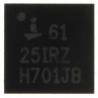
ISL6125IRZA Intersil, ISL6125IRZA Datasheet - Page 4

ISL6125IRZA
Manufacturer Part Number
ISL6125IRZA
Description
IC POWER SUPPLY SEQUENCER 24QFN
Manufacturer
Intersil
Datasheet
1.ISL6123IRZA.pdf
(22 pages)
Specifications of ISL6125IRZA
Applications
Power Supply Sequencer
Voltage - Supply
1.5 V ~ 5.5 V
Current - Supply
200µA
Operating Temperature
-40°C ~ 85°C
Mounting Type
Surface Mount
Package / Case
24-VQFN
Lead Free Status / RoHS Status
Lead free / RoHS Compliant
Voltage - Input
-
Pin Descriptions
DLY_OFF_C
DLY_OFF_D
DLY_OFF_A
DLY_OFF_B
ENABLE_1/
ENABLE_2/
DLY_ON_A
DLY_ON_B
DLY_ON_C
DLY_ON_D
ENABLE_1
ENABLE_2
RESET_2
UVLO_A
UVLO_B
UVLO_C
UVLO_D
GATE_C
GATE_D
SYSRST
GATE_A
GATE_B
RESET
NAME
VDD
GND
GND
PIN
NC
ISL6123, ISL6124,
ISL6125
EPAD
9, 19
NC
NC
23
10
24
20
12
17
14
21
16
15
18
13
22
1
8
3
4
2
5
6
7
ISL6123, ISL6124, ISL6125, ISL6126, ISL6127, ISL6128, ISL6130
PIN NUMBER
4
15, 16, 19,
ISL6126,
ISL6130
8, 9, 11,
EPAD
21, 22
NC
NC
23
10
24
20
12
17
14
18
13
1
3
4
2
5
6
7
-
-
-
-
-
3, 4, 8, 9,
15,16,18,
ISL6127
11, 13,
19, 21
EPAD
NC
NC
23
10
24
20
12
17
14
22
1
2
5
6
7
-
-
-
-
-
-
-
-
ISL6128
19, 22
EPAD
23
10
11
24
20
12
17
14
21
16
15
18
13
1
9
8
3
4
2
5
6
7
-
Chip Bias. Bias IC from nominal 1.5V to 5V
Bias Return. IC ground
Input to start on/off sequencing. Input to initiate the start of the programmed
sequencing of supplies on or off. Enable functionality is disabled for 10ms
after UVLO is satisfied. ISL6123 and ISL6130 have ENABLE. ISL6124,
ISL6125, ISL6126 and ISL6127 have ENABLE. Only ISL6128 has 2 ENABLE
inputs; 1 for each 2 channel grouping. ENABLE_1 for (A, B), and ENABLE_2
for (C, D).
RESET Output. RESET provides a low signal 150ms after all GATEs are fully
enhanced. This delay is for stabilization of output voltages. RESET will assert
low upon UVLO not being satisfied or ENABLE/ENABLE being deasserted.
The RESET outputs are open drain N-channel FET and is guaranteed to be
in the correct state for VDD down to 1V and is filtered to ignore fast transients
on VDD and UVLO_X.
RESET_2 only exists on ISL6128 for (C, D) group I/O.
Undervoltage Lock Out/Monitoring Input. These inputs provide for a
programmable UV lockout referenced to an internal 0.633V reference and
are filtered to ignore short (<30µs) transients below programmed UVLO level.
Gate On Delay Timer Output. Allows for programming the delay and
sequence for VOUT turn-on using a capacitor to ground. Each capacitor is
charged with 1µA, 10ms after turn-on initiated by ENABLE/ENABLE with an
internal current source providing delay to the associated FETs GATE turn-on.
Gate Off Delay Timer Output. Allows for programming the delay and
sequence for VOUT turn-off through ENABLE/ENABLE via a capacitor to
ground. Each capacitor is charged with a 1µA internal current source to an
internal reference voltage causing the corresponding gate to be pulled down
turning-off the FET.
FET Gate Drive Output. Drives the external FETs with a 1µA current source
to soft-start ramp into the load.
On the ISL6125 only, these are open drain outputs that can be pulled up to a
maximum of VDD voltage.
System Reset I/O. As an input, allows for immediate and unconditional latch-off
of all GATE outputs when driven low. This input can also be used to initiate the
programmed sequence with ‘zero’ wait (no 10ms stabilization delay) from input
signal on this pin being driven high to first GATE. As an output when there is a
UV condition, this pin pulls low. If common to other SYSRST pins in a multiple IC
configuration, it will cause immediate and unconditional latch-off of all other
GATEs on all other ISL612X sequencers.
Ground. Die Substrate
No Connect
DESCRIPTION
October 15, 2008
FN9005.10


