L6610D STMicroelectronics, L6610D Datasheet - Page 5
L6610D
Manufacturer Part Number
L6610D
Description
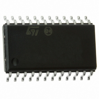
IC CTRLR HOUSEKEEPING BCD 24SOIC
Manufacturer
STMicroelectronics
Datasheet
1.L6610DTR.pdf
(29 pages)
Specifications of L6610D
Applications
Programmable Housekeeping Controller
Voltage - Supply
4.2 V ~ 7 V
Current - Supply
5mA
Operating Temperature
0°C ~ 105°C
Mounting Type
Surface Mount
Package / Case
24-SOIC (7.5mm Width)
Lead Free Status / RoHS Status
Lead free / RoHS Compliant
Voltage - Input
-
Available stocks
Company
Part Number
Manufacturer
Quantity
Price

Part Number:
L6610D
Manufacturer:
ST
Quantity:
20 000


PIN DESCRIPTION (continued)
FUNCTION DESCRIPTION
Pin #
PW-OK delay
17
18
19
20
21
22
23
24
OFF delay
Name
OCP
UVB
OVP
UVP
PROG
Name
GND
GND
-12V
3V3
12V
-5V
5V
Whenever one of the Main output voltages is detected going above its own OVP threshold, this
function set MFAULT (#1) high latching the outputs off. The latch is released after cycling PS-ON
(#15) switch or by reducing Vdd (#12) below the UV threshold.
Whenever one of the Main output voltages is detected going under its own UVP threshold, this
function sets MFAULT (#1) high; if latch mode has been selected, this function will be latched.
Otherwise an attempt will be made to restart the device after 1 second delay. If ACsns (#13) is
low due to a brownout condition, UVP is disabled.
Whenever either the 5V (or 3V3, digitally selectable) or the 12V output experiences an
overcurrent condition, the OCP function will force MFAULT (#1) high. If latch mode has been
selected, this condition will be latched otherwise an attempt is made to restart the supply after a
wait of 1 second.
Undervoltage blanking. When either converter is enabled, the relevant UV/OC monitoring circuits
must not intervene to allow all outputs to come within tolerance. 64 ms timing is provided; for the
auxiliary converter the timing starts as the IC has a valid supply, for the main converter it starts
as the ACsns pin detects a valid input voltage for the converter.
PW-OK delay. After power-up, when the all of the monitored voltages are above their own UV
threshold the PW-OK pin (#14) will be kept low for additional 250ms (typ.) to make sure all the
outputs are settled.
Power-off delay. As soon as PS-ON (#15) pin is recognized high, indicating an imminent turn-off
condition, PW-OK (#14) pin will go low immediately . The converter will be turned off after a
delay of 2.5ms.
-12V UV/OV monitor. If connected to a voltage greater than 1.5V (e.g. VREF, #16), the function
will be disabled.
-5V UV/OV monitor. If connected to a voltage greater than 1.5V (e.g. VREF, #16), the function will
be disabled.
Ground pin. The connection integrity of this pin is constantly monitored and in case of either a
bond wire or a PCB trace going open, MFAULT (#1) and DFAULT (#11) will be forced high
switching off the supply.
Ground pin. See above.
The chip has 2 operating modes, depending on PROG input pin biasing:
– normal mod e: PROG should be floating or shorted to ground;
– programming mod e: forcing PROG high (+5V), the chip enters programming mode. PW_OK
3V3 UV/OV monitor. It uses a separate reference to the feedback reference.
Input pin for 5V feedback, 5V current sense and 5V UV/OV monitor. 5V UV/OV uses a reference
separate from that used for feedback. This pin connects the 5V part of the Main error amplifier
feedback divider.
Input pin for 12V feedback, 12V current sense and 12V UV/OV monitor.12V UV/OV uses a
reference separate from that used for feedback. This pin connects the 12V part of the Main error
amplifier feedback divider.
(#14) and PS_ON (#15) pins are disconnected from their normal functionality and they become
inputs for DATA and CLOCK allowing the chip to be programmed. The programming mode al-
lows selecting some options and adjusting some setpoints;
Description
Description
L6610
5/29
Related parts for L6610D
Image
Part Number
Description
Manufacturer
Datasheet
Request
R

Part Number:
Description:
DIGITALLY PROGRAMMABLE SECONDARY HOUSEKEEPING CONTROLLER
Manufacturer:
STMicroelectronics
Datasheet:
Part Number:
Description:
STMicroelectronics [RIPPLE-CARRY BINARY COUNTER/DIVIDERS]
Manufacturer:
STMicroelectronics
Datasheet:
Part Number:
Description:
STMicroelectronics [LIQUID-CRYSTAL DISPLAY DRIVERS]
Manufacturer:
STMicroelectronics
Datasheet:

Part Number:
Description:
BOARD EVAL FOR MEMS SENSORS
Manufacturer:
STMicroelectronics
Datasheet:
Part Number:
Description:
NPN TRANSISTOR POWER MODULE
Manufacturer:
STMicroelectronics
Datasheet:
Part Number:
Description:
TURBOSWITCH ULTRA-FAST HIGH VOLTAGE DIODE
Manufacturer:
STMicroelectronics
Datasheet:
Part Number:
Description:
Manufacturer:
STMicroelectronics
Datasheet:
Part Number:
Description:
DIODE / SCR MODULE
Manufacturer:
STMicroelectronics
Datasheet:
Part Number:
Description:
DIODE / SCR MODULE
Manufacturer:
STMicroelectronics
Datasheet:
Part Number:
Description:
Search -----> STE16N100
Manufacturer:
STMicroelectronics
Datasheet:
Part Number:
Description:
Search ---> STE53NA50
Manufacturer:
STMicroelectronics
Datasheet:
Part Number:
Description:
NPN Transistor Power Module
Manufacturer:
STMicroelectronics
Datasheet: