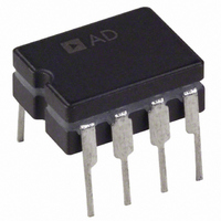
AD737AQ Analog Devices Inc, AD737AQ Datasheet

AD737AQ
Specifications of AD737AQ
Available stocks
Related parts for AD737AQ
AD737AQ Summary of contents
Page 1
FEATURES Computes True rms value Average rectified value Absolute value Provides 200 mV full-scale input range (larger inputs with input attenuator) Direct interfacing with 3½ digit CMOS ADCs 12 High input impedance: 10 Ω Low input bias current ...
Page 2
AD737 TABLE OF CONTENTS Features .............................................................................................. 1 Functional Block Diagram .............................................................. 1 General Description ......................................................................... 1 Product Highlights ........................................................................... 1 Revision History ............................................................................... 2 Specifications ..................................................................................... 3 Absolute Maximum Ratings ............................................................ 6 Thermal Resistance ...................................................................... 6 ESD Caution .................................................................................. 6 ...
Page 3
SPECIFICATIONS T = 25°C, ±V = ±5 V except as noted Specifications shown in boldface are tested on all production units at final electrical test. Results from these tests are used to calculate outgoing quality levels. Table ...
Page 4
AD737 Parameter Conditions Peak Transient ±V = +2.5 V input to S Input Pin 1 ±V = +2.8 V/−3 ±V = ± ±V = ±16 Input Resistance Input Bias ±V = ± ...
Page 5
Parameter Conditions 3 dB Bandwidth rms rms 100 mV rms 200 mV rms IN Low-Z Input (Pin 1) 1% Additional rms ...
Page 6
AD737 ABSOLUTE MAXIMUM RATINGS Table 2. Parameter Supply Voltage Internal Power Dissipation Input Voltage Output Short-Circuit Duration Differential Input Voltage Storage Temperature Range CERDIP (Q-8) PDIP (N-8) and SOIC_N (R-8) Lead Temperature, Soldering (60 sec) ESD Rating Stresses above those ...
Page 7
PIN CONFIGURATIONS AND FUNCTION DESCRIPTIONS C COM AD737 POWER DOWN OUTPUT 3 TOP VIEW 6 (Not to Scale) – Figure 2. SOIC_N Pin Configuration (R-8) Table ...
Page 8
AD737 TYPICAL PERFORMANCE CHARACTERISTICS T = 25°C, ±V = ±5 V (except AD737J-5, where ± unless otherwise specified. 0 200mV rms 100µ 22µF F 0.3 0.1 0 –0.1 –0.3 ...
Page 9
V = 200mV rms 100µ 22µF F 0.4 0.2 0 –0.2 –0.4 –0.6 –0.8 –60 –40 – TEMPERATURE (°C) Figure 11. Additional Error vs. Temperature 500 400 ...
Page 10
AD737 4.0 3.5 3.0 2.5 2.0 1.5 1 SUPPLY VOLTAGE (±V) Figure 17. Input Bias Current vs. Supply Voltage 1V 100mV C = 10µF AV 10mV C = 33µF AV 1mV 100µV 1ms 10ms 100ms ...
Page 11
V = ±2.5V 22µ 4.7µ 22µ 100mV 0.5% 10mV 10% 1mV –3dB 1% 100µV 0 FREQUENCY (kHz) Figure 21. Error Contours Driving Pin ...
Page 12
AD737 THEORY OF OPERATION As shown in Figure 24, the AD737 has four functional subsec- tions: an input amplifier, a full-wave rectifier, an rms core, and a bias section. The FET input amplifier allows a high impedance, buffered input at ...
Page 13
DC ERROR, OUTPUT RIPPLE, AND AVERAGING ERROR Figure 25 shows the typical output waveform of the AD737 with a sine wave input voltage applied. As with all real-world devices, the ideal output never exactly achieved; ...
Page 14
AD737 APPLICATIONS INFORMATION RMS MEASUREMENT—CHOOSING AN OPTIMUM VALUE FOR C AV Because the external averaging capacitor, C tified input signal during rms computation, its value directly affects the accuracy of the rms measurement, especially at low frequencies. Furthermore, because the ...
Page 15
Battery Operation All the level-shifting for battery operation is provided by the 3½ digit converter, shown in Figure 28. Alternatively, an external op amp adds flexibility by accommodating nonzero common-mode voltages and providing output scaling and offset to zero. When ...
Page 16
AD737 SWITCH CLOSED ACTIVATES POWER-DOWN MODE. AD737 DRAWS JUST 40µA IN THIS MODE 1PRV 0.01µF V 200mV IN 1N4148 9MΩ 2V 900kΩ 47kΩ 20V 1W 1N4148 90kΩ 200V POWER 10kΩ 1µF + INPUT SCALE FACTOR ADJ 69.8kΩ ...
Page 17
C C 10µ AD737 8kΩ COM FULL-WAVE RECTIFIER 8kΩ INPUT AMPLIFIER POWER BIAS 3 DOWN SECTION –V S RMS 4 CORE + R1** CAL CONNECT *Q1, ...
Page 18
AD737 AD737 EVALUATION BOARD An evaluation board, AD737-EVALZ, is available for experi- ments or for becoming familiar with rms-to-dc converters. Figure photograph of the board; Figure 35 to Figure 38 show the signal and power plane copper ...
Page 19
Table 7. AD737 Evaluation Board Bill of Materials Qty Name Description 1 Test loop Red 1 Test loop Green 2 Capacitor Tantalum 10 μ Capacitor 0.1 μ 0603, X7R 1 Capacitor Tantalum ...
Page 20
AD737 OUTLINE DIMENSIONS COPLANARITY 5.00 (0.1968) 4.80 (0.1890 6.20 (0.2441) 4.00 (0.1574) 1 5.80 (0.2284) 3.80 (0.1497) 4 1.27 (0.0500) BSC 1.75 (0.0688) 1.35 (0.0532) 0.25 (0.0098) 8° 0.10 (0.0040) 0° 0.51 (0.0201) 0.10 0.31 (0.0122) 0.25 (0.0098) ...
Page 21
BSC 0.210 (5.33) MAX 0.015 0.150 (3.81) (0.38) 0.015 (0.38) MIN 0.130 (3.30) 0.115 (2.92) SEATING PLANE 0.022 (0.56) 0.005 (0.13) 0.018 ...
Page 22
... AD737 ORDERING GUIDE Model Temperature Range AD737AN −40°C to +85°C 1 AD737ANZ −40°C to +85°C AD737AQ −40°C to +85°C AD737AR −40°C to +85°C 1 AD737ARZ −40°C to +85°C AD737BQ −40°C to +85°C AD737JN 0°C to 70°C 1 AD737JNZ 0° ...
Page 23
NOTES Rev Page AD737 ...
Page 24
AD737 NOTES ©2008 Analog Devices, Inc. All rights reserved. Trademarks and registered trademarks are the property of their respective owners. D00828-0-10/08(H) Rev Page ...


