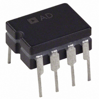
AD737AQ Analog Devices Inc, AD737AQ Datasheet - Page 13

AD737AQ
Manufacturer Part Number
AD737AQ
Description
IC AC RMS TO DC CONV 5V 8-CDIP
Manufacturer
Analog Devices Inc
Datasheet
1.AD737JNZ.pdf
(24 pages)
Specifications of AD737AQ
Rohs Status
RoHS non-compliant
Current - Supply
170mA
Voltage - Supply
±5.0V
Mounting Type
Through Hole
Package / Case
8-CDIP (0.300", 7.62mm)
For Use With
AD737-EVALZ - BOARD EVALUATION FOR AD737
Available stocks
Company
Part Number
Manufacturer
Quantity
Price
Part Number:
AD737AQ
Manufacturer:
ADI/亚德诺
Quantity:
20 000
DC ERROR, OUTPUT RIPPLE, AND
AVERAGING ERROR
Figure 25 shows the typical output waveform of the AD737 with
a sine wave input voltage applied. As with all real-world devices,
the ideal output of V
the output contains both a dc and an ac error component.
As shown, the dc error is the difference between the average of
the output signal (when all the ripple in the output has been
removed by external filtering) and the ideal dc output. The dc
error component is, therefore, set solely by the value of the
averaging capacitor used—no amount of post filtering (using a
very large postfiltering capacitor, C
to equal its ideal value. The ac error component, an output
ripple, can be easily removed using a large enough C
In most cases, the combined magnitudes of the dc and ac error
components must be considered when selecting appropriate
values for C
senting the maximum uncertainty of the measurement, is
termed the averaging error and is equal to the peak value of the
output ripple plus the dc error. As the input frequency increases,
both error components decrease rapidly. If the input frequency
doubles, the dc error and ripple reduce to one-quarter and
one-half of their original values, respectively, and rapidly
become insignificant.
Table 5. Error Introduced by an Average Responding Circuit When Measuring Common Waveforms
Type of Waveform
1 V Peak Amplitude
Undistorted Sine Wave
Symmetrical Square Wave
Undistorted Triangle Wave
Gaussian Noise (98% of
Peaks <1 V)
Rectangular
Pulse Train
SCR Waveforms
50% Duty Cycle
25% Duty Cycle
Figure 25. Output Waveform for Sine Wave Input Voltage
E
O
AV
and C
DOUBLE-FREQUENCY
F
OUT
capacitors. This combined error, repre-
IDEAL
E
= V
O
RIPPLE
DC ERROR = E
IN
Crest Factor
(V
1.414
1.00
1.73
3
2
10
2
4.7
is never exactly achieved; instead,
PEAK
/V rms)
F
) allows the output voltage
AVERAGE E
O
– E
O
(IDEAL)
O
= E
TIME
O
True RMS
Value (V)
0.707
1.00
0.577
0.333
0.5
0.1
0.495
0.212
F
.
Rev. H | Page 13 of 24
0.295
0.354
Reading of an Average Responding Circuit Calibrated to
an RMS Sine Wave Value (V)
0.707
1.11
0.555
0.278
0.011
0.150
AC MEASUREMENT ACCURACY AND
CREST FACTOR
The crest factor of the input waveform is often overlooked when
determining the accuracy of an ac measurement. Crest factor is
defined as the ratio of the peak signal amplitude to the rms
amplitude (crest factor = V
waveforms, such as sine and triangle waves, have relatively low
crest factors (≥2). Other waveforms, such as low duty cycle
pulse trains and SCR waveforms, have high crest factors. These
types of waveforms require a long averaging time constant to
average out the long time periods between pulses. Figure 10
shows the additional error vs. the crest factor of the AD737 for
various values of C
CALCULATING SETTLING TIME
Figure 18 can be used to closely approximate the time required
for the AD737 to settle when its input level is reduced in
amplitude. The net time required for the rms converter to settle
is the difference between two times extracted from the graph:
the initial time minus the final settling time. As an example,
consider the following conditions: a 33 μF averaging capacitor,
an initial rms input level of 100 mV, and a final (reduced) input
level of 1 mV. From Figure 18, the initial settling time (where
the 100 mV line intersects the 33 μF line) is approximately
80 ms. The settling time corresponding to the new or final input
level of 1 mV is approximately 8 seconds. Therefore, the net
time for the circuit to settle to its new value is 8 seconds minus
80 ms, which is 7.92 seconds.
Note that, because of the inherent smoothness of the decay
characteristic of a capacitor/diode combination, this is the total
settling time to the final value (not the settling time to 1%,
0.1%, and so on, of the final value). Also, this graph provides
the worst-case settling time because the AD737 settles very
quickly with increasing input levels.
AV
.
PEAK
/V rms). Many common
AD737
Error (%)
0
11.0
−3.8
−11.4
−44
−89
−28
−30


