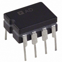
AD737AQ Analog Devices Inc, AD737AQ Datasheet - Page 14

AD737AQ
Manufacturer Part Number
AD737AQ
Description
IC AC RMS TO DC CONV 5V 8-CDIP
Manufacturer
Analog Devices Inc
Datasheet
1.AD737JNZ.pdf
(24 pages)
Specifications of AD737AQ
Rohs Status
RoHS non-compliant
Current - Supply
170mA
Voltage - Supply
±5.0V
Mounting Type
Through Hole
Package / Case
8-CDIP (0.300", 7.62mm)
For Use With
AD737-EVALZ - BOARD EVALUATION FOR AD737
Available stocks
Company
Part Number
Manufacturer
Quantity
Price
Part Number:
AD737AQ
Manufacturer:
ADI/亚德诺
Quantity:
20 000
AD737
APPLICATIONS INFORMATION
RMS MEASUREMENT—CHOOSING AN OPTIMUM
VALUE FOR C
Because the external averaging capacitor, C
tified input signal during rms computation, its value directly
affects the accuracy of the rms measurement, especially at low
frequencies. Furthermore, because the averaging capacitor is
connected across a diode in the rms core, the averaging time
constant (τ
decreases. It follows that decreasing the input signal decreases
errors due to nonideal averaging but increases the settling time
approaching the decreased rms-computed dc value. Thus,
diminishing input values allow the circuit to perform better
(due to increased averaging) while increasing the waiting time
between measurements. A trade-off must be made between
computational accuracy and settling time when selecting C
RAPID SETTLING TIMES VIA THE AVERAGE
RESPONDING CONNECTION
Because the average responding connection shown in Figure 26
does not use an averaging capacitor, its settling time does not vary
with input signal level; it is determined solely by the RC time
constant of C
Selectable Average or RMS Conversion
For some applications, it is desirable to be able to select between
rms-value-to-dc conversion and average-value-to-dc conversion.
If C
wave rectifier is a highly accurate absolute value circuit. A CMOS
switch whose gate is controlled by a logic level selects between
average and rms values.
POWER
V
DOWN
AV
IN
C
–V
C
is disconnected from the root-mean core, the AD737 full-
S
1
2
3
4
AV
NEGATIVE SUPPLY
8kΩ
POSITIVE SUPPLY
) increases exponentially as the input signal
F
Figure 26. AD737 Average Responding Circuit
and the internal 8 kΩ output scaling resistor.
SECTION
BIAS
AMPLIFIER
AV
INPUT
COMMON
FULL-WAVE
RECTIFIER
CORE
RMS
AD737
0.1µF
0.1µF
8kΩ
AV
8
7
6
5
COM
OUTPUT
–V
+V
, holds the rec-
+V
C
S
S
AV
S
+
C
33µF
F
V
OUT
AV
Rev. H | Page 14 of 24
.
SELECTING PRACTICAL VALUES FOR CAPACITORS
Table 6 provides practical values of C
common applications.
The input coupling capacitor, C
internal input scaling resistor, determines the −3 dB low frequency
roll-off. This frequency, F
Note that, at F
(−3 dB) of reading. To reduce this error to 0.5% of reading,
choose a value of C
frequency to be measured.
In addition, if the input voltage has more than 100 mV of dc
offset, the ac coupling network at Pin 2 is required in addition
to Capacitor C
SCALING INPUT AND OUTPUT VOLTAGES
The AD737 is an extremely flexible device. With minimal
external circuitry, it can be powered with single- or dual-
polarity power supplies, and input and output voltages are
independently scalable to accommodate nonmatching I/O
devices. This section describes a few such applications.
Extending or Scaling the Input Range
For low supply voltage applications, the maximum peak voltage
to the device is extended by simply applying the input voltage to
Pin 1 across the internal 8 kΩ input resistor. The AD737 input
circuit functions quasi-differentially, with a high impedance
FET input at Pin 2 (noninverting) and a low impedance input at
Pin 1 (inverting, see Figure 26). The internal 8 kΩ resistor behaves
as a voltage-to-current converter connected to the summing
node of a feedback loop around the input amplifier. Because the
feedback loop acts to servo the summing node voltage to match
the voltage at Pin 2, the maximum peak input voltage increases
until the internal circuit runs out of headroom, approximately
double for a symmetrical dual supply.
Figure 27. CMOS Switch Is Used to Select RMS or Average Responding Modes
VIN
RMS
F
L
=
2
1MΩ
π
×
–2.5V
L
C
, the amplitude error is approximately −30%
8000
.
1
2
3
4
CC
V
–V
C
IN
×
S
that sets F
AD737
NTR4501NT1
C
1
C
L
(
, is equal to
OUT
in
COM
+V
C
33µF
AV
Farads
S
C
, in conjunction with the 8 kΩ
L
8
7
6
5
at one-tenth of the lowest
)
AV
and C
33µF
rms
AVG
F
for several
+2.5V
VOUT
ASSUMED TO
BE A LOGIC
SOURCE
DC
(1)


