LM96080CIMT/NOPB National Semiconductor, LM96080CIMT/NOPB Datasheet - Page 7
LM96080CIMT/NOPB
Manufacturer Part Number
LM96080CIMT/NOPB
Description
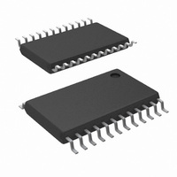
IC HARDWARE MONITOR 24-TSSOP
Manufacturer
National Semiconductor
Series
PowerWise®r
Datasheet
1.LM96080CIMTNOPB.pdf
(30 pages)
Specifications of LM96080CIMT/NOPB
Function
Hardware Monitor
Topology
ADC (Sigma Delta), Comparator, Fan Speed Counter, Register Bank
Sensor Type
External & Internal
Sensing Temperature
-40°C ~ 125°C, External Sensor
Output Type
I²C™
Output Alarm
No
Output Fan
Yes
Voltage - Supply
3 V ~ 5.5 V
Operating Temperature
-40°C ~ 125°C
Mounting Type
Surface Mount
Package / Case
24-TSSOP
Lead Free Status / RoHS Status
Lead free / RoHS Compliant
Other names
LM96080CIM
Available stocks
Company
Part Number
Manufacturer
Quantity
Price
Company:

Part Number:
LM96080CIMT/NOPB
Manufacturer:
National Semiconductor
Quantity:
135
Company:
Part Number:
LM96080CIMT/NOPB
Manufacturer:
NS
Quantity:
175


SERIAL BUS TIMING CHARACTERISTICS
Symbol
t
TIMEOUT
AC Electrical Characteristics
The following specifications apply for +3.0 V
= T
Note 1: Absolute Maximum Ratings indicate limits beyond which damage to the device may occur. Operating Ratings indicate conditions for which the device is
functional, but do not guarantee specific performance limits. For guaranteed specifications and test conditions, see the Electrical Characteristics. The guaranteed
specifications apply only for the test conditions listed. Some performance characteristics may degrade when the device is not operated under the listed test
conditions.
Note 2: All voltages are measured with respect to GND, unless otherwise specified
Note 3: When the input voltage (V
The 30 mA maximum package input current rating limits the number of pins that can safely exceed the power supplies with an input current of 5 mA to six pins.
Parasitic components and/or ESD protection circuitry are shown in the Pin Descriptions table.
Note 4: The maximum power dissipation must be derated at elevated temperatures and is dictated by T
allowable power dissipation at any temperature is P
Note 5: Human body model (HBM) is a charged 100 pF capacitor discharged into a 1.5 kΩ resistor. Machine model (MM), is a charged 200 pF capacitor discharged
directly into each pin. Charged Device Model (CDM) simulates a pin slowly acquiring charge (such as from a device sliding down the feeder in an automated
assembler) then rapidly being discharged.
Note 6: Reflow temperature profiles are different for packages containing lead (Pb) than for those that do not..
Note 7: Each input and output is protected by an ESD structure to GND, as shown in the Pin Descriptions table. Input voltage magnitude up to 0.3V above V
0.3V below GND will not damage the LM96080. There are parasitic diodes that exist between some inputs and the power supply rails. Errors in the ADC conversion
can occur if these diodes are forward biased by more than 50 mV. As an example, if V
conversions.
Note 8: Typicals are at T
Note 9: Limits are guaranteed to National's AOQL (Average Outgoing Quality Level).
Note 10: TUE (Total Unadjusted Error) includes Offset, Gain and Linearity errors of the ADC.
Note 11: Limit is guaranteed by Design.
Note 12: Total Monitoring Cycle Time includes temperature conversion, 7 analog input voltage conversions and 2 tachometer readings. For more information
on the conversion rates, refer to the description of bit 0, register 07h in section 13.0: Registers and RAM.
Note 13: The total fan count is based on 2 pulses per revolution of the fan tachometer output.
Note 14: Timing specifications are tested at the Serial Bus Input logic levels, V
SCL and SDA edge rates are similar.
t
t
t
t
t
1
2
3
4
5
MIN
to T
SCL (Clock) Period
Data In Setup Time to SCL High
Data Out Stable After SCL Low
SDA Low Setup Time to SCL Low (start)
SDA High Hold Time After SCL High (stop)
SCL or SDA time low for I
MAX
; all other limits T
J
= T
A
= 25°C and represent most likely parametric norm.
IN
) at any pin exceeds the power supplies (V
A
= T
Parameter
2
C bus reset
J
= 25°C.
D
= (T
FIGURE 1. Serial Bus Timing Diagram
DC
J
(Note
≤
max−T
V
+
≤
14)
A
)/θ
+5.5 V
JA
.
DC
IN
IN(0)
7
, unless otherwise specified. Boldface limits apply for T
< (GND or GNDA) or V
= 0.3 × V
+
is 4.50 V
Conditions
+
for a falling edge and V
DC
, input voltage must be
J
max, θ
IN
>V
+
JA
), the current at that pin should be limited to 5 mA.
and the ambient temperature, T
(Note
Typical
IN(1)
8)
= 0.7 × V
≤
4.55 V
(Note
+
Limits
DC
for a rising edge when the
100
100
100
100
2.5
25
35
, to ensure accurate
0
30070126
9)
A
. The maximum
www.national.com
ms (max)
μs (max)
ms (min)
(Limits)
μs (min)
ns (min)
ns (min)
ns (min)
ns (min)
Units
A
= T
+
J
or
Related parts for LM96080CIMT/NOPB
Image
Part Number
Description
Manufacturer
Datasheet
Request
R

Part Number:
Description:
National Semiconductor [8-Bit D/A Converter]
Manufacturer:
National Semiconductor
Datasheet:
Part Number:
Description:
National Semiconductor [Media Coprocessor]
Manufacturer:
National Semiconductor
Datasheet:
Part Number:
Description:
Digitally Controlled Tone and Volume Circuit with Stereo Audio Power Amplifier, Microphone Preamp Stage and National 3D Sound
Manufacturer:
National Semiconductor
Datasheet:
Part Number:
Description:
Digitally Controlled Tone and Volume Circuit with Stereo Audio Power Amplifier, Microphone Preamp Stage and National 3D Sound
Manufacturer:
National Semiconductor
Datasheet:
Part Number:
Description:
AC97 Rev 2 Codec with Sample Rate Conversion and National 3D Sound
Manufacturer:
National Semiconductor
Part Number:
Description:
Manufacturer:
National Semiconductor
Datasheet:
Part Number:
Description:
Manufacturer:
National Semiconductor
Datasheet:
Part Number:
Description:
General Purpose, Low Voltage, Low Power, Rail-to-Rail Output Operational Amplifiers
Manufacturer:
National Semiconductor
Datasheet:
Part Number:
Description:
8-bit 20 MSPS flash A/D converter.
Manufacturer:
National Semiconductor
Datasheet:
Part Number:
Description:
Low Noise Quad Operational Amplifier
Manufacturer:
National Semiconductor
Datasheet:
Part Number:
Description:
Quad Differential Line Receivers
Manufacturer:
National Semiconductor
Datasheet:
Part Number:
Description:
Quad High Speed Trapezoidal? Bus Transceiver
Manufacturer:
National Semiconductor
Datasheet:
Part Number:
Description:
Dual Line Receiver
Manufacturer:
National Semiconductor
Datasheet:
Part Number:
Description:
TTL to 10k ECL Level Translator with Latch
Manufacturer:
National Semiconductor
Datasheet: