TL431ASDT,215 NXP Semiconductors, TL431ASDT,215 Datasheet
TL431ASDT,215
Specifications of TL431ASDT,215
935288351215


Related parts for TL431ASDT,215


TL431ASDT,215 Summary of contents
Page 1
TL431 family Adjustable precision shunt regulator Rev. 3 — 5 November 2010 1. General description Three-terminal shunt regulator family with an output voltage range between set by two external resistors. • The TL431xDBZR types feature an enhanced ...
Page 2
... NXP Semiconductors 2. Features and benefits Programmable output voltage Three different reference voltage tolerances: Standard grade A-Grade B-Grade: 0.5 % Typical temperature drift (in a range of 0 ° °C) Low output noise Typical output impedance: 0.2 Ω Sink current capability 100 mA AEC-Q100 qualified (grade 1) 3 ...
Page 3
... NXP Semiconductors 5. Ordering information Table 3. Type number TL431CDBZR TL431IDBZR TL431QDBZR TL431FDT TL431MFDT TL431SDT TL431MSDT TL431ACDBZR TL431AIDBZR TL431AQDBZR TL431AFDT TL431AMFDT TL431ASDT TL431AMSDT TL431BCDBZR TL431BIDBZR TL431BQDBZR TL431BFDT TL431BMFDT TL431BSDT TL431BMSDT TL431_FAM Product data sheet Ordering information Package Name Description - plastic surface-mounted package; 3 leads All information provided in this document is subject to legal disclaimers. Rev. 3 — ...
Page 4
... NXP Semiconductors 6. Marking Table 4. Type number TL431CDBZR TL431IDBZR TL431QDBZR TL431FDT TL431MFDT TL431SDT TL431MSDT TL431ACDBZR TL431AIDBZR TL431AQDBZR TL431AFDT TL431AMFDT [ placeholder for manufacturing site code 7. Functional diagram The TL431 family comprises a range of 3-terminal adjustable shunt regulators, with specified thermal stability over applicable automotive and commercial temperature ranges ...
Page 5
... NXP Semiconductors 8. Pinning information Table 5. Pin Normal pinning: All types without MFDT and MSDT ending Mirrored pinning: All types with MFDT and MSDT ending Limiting values Table 6. In accordance with the Absolute Maximum Rating System (IEC 60134). Symbol ref P tot amb ...
Page 6
... NXP Semiconductors (1) Ceramic PCB, Al (2) FR4 PCB, mounting pad for anode 1 cm (3) FR4 PCB, standard footprint Fig 2. Table amb Symbol V ESD 10. Recommended operating conditions Table 8. Symbol TL431_FAM Product data sheet 1250 P tot (mW) (1) 1000 750 (2) 500 (3) 250 0 −75 − standard footprint ...
Page 7
... NXP Semiconductors 11. Thermal characteristics Table 9. Symbol R th(j-a) R th(j-sp) [1] Device mounted on an FR4 PCB, single-sided copper, tin-plated and standard footprint. [2] Device mounted on an FR4 PCB, single-sided copper, tin-plated, mounting pad for anode 1 cm [3] Device mounted on a ceramic PCB, Al [4] Soldering point of anode. ...
Page 8
... NXP Semiconductors Table 10. Characteristics …continued Symbol Parameter I off-state current off Z dynamic cathode-anode KA impedance A-Grade (1 %): TL431ACDBZR; TL431AIDBZR; TL431AQDBZR; TL431AFDT; TL431AMFDT; TL431ASDT; TL431AMSDT V reference voltage ref ΔV reference voltage variation ref TL431ACDBZR TL431AIDBZR TL431AQDBZR TL431AFDT TL431AMFDT TL431ASDT TL431AMSDT ΔV /ΔV reference voltage variation ...
Page 9
... NXP Semiconductors Table 10. Characteristics …continued Symbol Parameter B-Grade (0.5 %): TL431BCDBZR; TL431BIDBZR; TL431BQDBZR; TL431BFDT; TL431BMFDT; TL431BSDT; TL431BMSDT V reference voltage ref ΔV reference voltage variation ref TL431BCDBZR TL431BIDBZR TL431BQDBZR TL431BFDT TL431BMFDT TL431BSDT TL431BMSDT ΔV /ΔV reference voltage variation ref KA to cathode-anode voltage variation ratio ...
Page 10
... NXP Semiconductors 2.60 V ref (V) 2.56 2.52 2.48 2.44 2.40 −75 − mA ref Fig 3. Reference voltage as a function of ambient temperature; typical values mA ref Fig 5. Test circuit to Figure 3 TL431_FAM Product data sheet 006aab571 (mA) 75 125 T (°C) amb Fig 4. INPUT V ref GND and Figure 4 All information provided in this document is subject to legal disclaimers. Rev. 3 — ...
Page 11
... NXP Semiconductors 5.0 I ref (μA) 4.0 3.0 2.0 1.0 0.0 −75 − mA kΩ open K Fig 6. Reference current as a function of ambient temperature; typical values ⎛ ⎞ R1 × ------ - ⎝ ⎠ KA ref R2 Fig 8. Test circuit to Figure 6 TL431_FAM Product data sheet 006aab574 ΔV (mV) ...
Page 12
... NXP Semiconductors Fig 9. Fig 10. Off-state current as a function of ambient temperature; test circuit TL431_FAM Product data sheet 250 I off (nA) 200 150 100 50 0 −75 − ref Off-state current as a function of ambient temperature; typical values INPUT ref All information provided in this document is subject to legal disclaimers. ...
Page 13
... NXP Semiconductors 6 ( out ( − °C T amb (1) Input (2) Output Fig 11. All types except TL431XFDT and TL431XSDT: Input voltage and output voltage as a function of time; typical values 6 ( out ( − °C T amb (1) Input (2) Output Fig 13. TL431XSDT: Input voltage and output voltage as a function of time ...
Page 14
... NXP Semiconductors (dB ° mA amb Fig 15. All types except TL431XFDT and TL431XSDT: Voltage amplification as a function of frequency; typical values (dB ° mA amb Fig 17. TL431XSDT: Voltage amplification as a function of frequency; typical values TL431_FAM Product data sheet 006aab583 (dB (kHz) Fig 16. TL431XFDT: 006aab582 (kHz) Fig 18. Test circuit to All information provided in this document is subject to legal disclaimers. Rev. 3 — ...
Page 15
... NXP Semiconductors (Ω − ° mA amb Fig 19. All types except TL431XFDT and TL431XSDT: Dynamic cathode-anode impedance as a function of frequency; typical values (Ω − ° mA amb Fig 21. TL431XSDT: Dynamic cathode-anode impedance as a function of frequency; typical values TL431_FAM Product data sheet 006aab585 2 10 ...
Page 16
... NXP Semiconductors 100 I K (mA Stable °C T amb ( ref oscillation oscillation oscillation KA Fig 23. All types except TL431XFDT and TL431XSDT: Cathode current as a function of load capacitance; typical values 150 Ω ref = 25 °C T amb Fig 24. Test circuit (1) to Figure 23 TL431_FAM Product data sheet (1) (1) ...
Page 17
... NXP Semiconductors 100 I K (mA − °C T amb ( ref oscillation oscillation oscillation KA Fig 26. TL431XFDT: Cathode current as a function of load capacitance; typical values 150 Ω ref = 25 °C T amb Fig 27. Test circuit (1) to Figure 26 TL431_FAM Product data sheet (1) Stable Oscillation 10 V BATT GND 006aab589 Fig 28 ...
Page 18
... NXP Semiconductors 100 I K (mA Stable − °C T amb ( ref ( oscillation oscillation KA Fig 29. TL431XSDT: Cathode current as a function of load capacitance; typical values 150 Ω ref = 25 °C T amb Fig 30. Test circuit (1) to Figure 29 TL431_FAM Product data sheet (1) (2) Oscillation 10 V BATT GND 006aab589 Fig 31 ...
Page 19
... NXP Semiconductors 13. Application information Fig 32. Shunt regulator Fig 33. Series pass regulator Fig 34. Single-supply comparator with temperature-compensated threshold TL431_FAM Product data sheet V+ ⎛ ⎞ R1 × ------ - ⎝ ⎠ OUT ref R2 V+ ⎛ ⎞ R1 × ------ - ⎝ ⎠ ( OUT ref OUT min ref < ⇒ > ...
Page 20
... NXP Semiconductors Fig 35. Constant current source Fig 36. High-current shunt regulator Fig 37. Constant current sink TL431_FAM Product data sheet V+ V ref --------- I = OUT ⎛ ⎞ R1 × ------ - ⎝ ⎠ OUT ref ref --------- I = SINK R S All information provided in this document is subject to legal disclaimers. Rev. 3 — 5 November 2010 ...
Page 21
... NXP Semiconductors Fig 38. TL431 in control loop of SMPS 14. Test information 14.1 Quality information This product has been qualified in accordance with the Automotive Electronics Council (AEC) standard Q100 - Failure mechanism based stress test qualification for integrated circuits, and is suitable for use in automotive applications. ...
Page 22
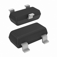
... NXP Semiconductors 15. Package outline Fig 39. Package outline SOT23 (TO-236AB) TL431_FAM Product data sheet 3.0 2.8 3 2.5 1.4 2.1 1.2 1 1.9 Dimensions in mm All information provided in this document is subject to legal disclaimers. Rev. 3 — 5 November 2010 TL431 family Adjustable precision shunt regulator 1.1 ...
Page 23
... NXP Semiconductors 16. Packing information Table 11. The indicated -xxx are the last three digits of the 12NC ordering code. Type number TL431CDBZR TL431IDBZR TL431QDBZR TL431FDT TL431MFDT TL431SDT TL431MSDT TL431ACDBZR TL431AIDBZR TL431AQDBZR TL431AFDT TL431AMFDT TL431ASDT TL431AMSDT TL431BCDBZR TL431BIDBZR TL431BQDBZR TL431BFDT TL431BMFDT TL431BSDT TL431BMSDT [1] For further information and the availability of packing methods, see ...
Page 24
... NXP Semiconductors 17. Soldering 3 1.7 Fig 40. Reflow soldering footprint SOT23 (TO-236AB) 2.6 4.6 Fig 41. Wave soldering footprint SOT23 (TO-236AB) TL431_FAM Product data sheet 3.3 2.9 1.9 0.7 (3×) 0.5 (3×) 0.6 (3×) 1 2.2 1.2 (2×) 1.4 (2×) 1.4 2.8 4.5 All information provided in this document is subject to legal disclaimers. ...
Page 25
... NXP Semiconductors 18. Revision history Table 12. Revision history Document ID Release date TL431_FAM_3 20101105 • Modifications: Type numbers TL431FDT, TL431MFDT, TL431AFDT, TL431AMFDT, TL431BFDT and TL431BMFDT added • Section 12 • Section 13 “Application • Section 19 “Legal TL431_FAM_2 20100120 TL431_FAM_1 20090806 TL431_FAM Product data sheet Data sheet status Product data sheet “ ...
Page 26
... In no event shall NXP Semiconductors be liable for any indirect, incidental, punitive, special or consequential damages (including - without limitation - lost profits, lost savings, business interruption, costs related to the removal or ...
Page 27
... NXP Semiconductors Quick reference data — The Quick reference data is an extract of the product data given in the Limiting values and Characteristics sections of this document, and as such is not complete, exhaustive or legally binding. 20. Contact information For more information, please visit: For sales office addresses, please send an email to: ...
Page 28
... NXP Semiconductors 21. Contents 1 General description . . . . . . . . . . . . . . . . . . . . . . 1 2 Features and benefits . . . . . . . . . . . . . . . . . . . . 2 3 Applications . . . . . . . . . . . . . . . . . . . . . . . . . . . . 2 4 Quick reference data . . . . . . . . . . . . . . . . . . . . . 2 5 Ordering information . . . . . . . . . . . . . . . . . . . . . 3 6 Marking . . . . . . . . . . . . . . . . . . . . . . . . . . . . . . . . 4 7 Functional diagram . . . . . . . . . . . . . . . . . . . . . . 4 8 Pinning information . . . . . . . . . . . . . . . . . . . . . . 5 9 Limiting values Recommended operating conditions Thermal characteristics . . . . . . . . . . . . . . . . . . 7 12 Characteristics . . . . . . . . . . . . . . . . . . . . . . . . . . 7 13 Application information Test information . . . . . . . . . . . . . . . . . . . . . . . . 21 14 ...