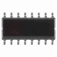
E-L5991AD STMicroelectronics, E-L5991AD Datasheet - Page 3

E-L5991AD
Manufacturer Part Number
E-L5991AD
Description
IC CTRLR PRIMARY W/STDBY 16-SOIC
Manufacturer
STMicroelectronics
Datasheet
1.L5991AD13TR.pdf
(23 pages)
Specifications of E-L5991AD
Mfg Application Notes
25W Off-Line Battery Charger with L5991A AppNote 300W Forward Converter with L5991A AppNote 45W AC-DC Adapter with Standby AppNote 60W Power Supply using the L5991 AppNote 80W Adapter using L6561/L5991A AppNote 90W SMPS for Monitors with Standby AppNote Trick Enhances L5991s Standby Function AppNote L5991-Based Converter, Temp Extra Power AppNote Auxiliary Power Supply Design AppNote Minimize Power Losses AppNote
Pwm Type
Current Mode
Number Of Outputs
1
Frequency - Max
1MHz
Duty Cycle
93%
Voltage - Supply
8.2 V ~ 20 V
Buck
No
Boost
Yes
Flyback
Yes
Inverting
No
Doubler
No
Divider
No
Cuk
No
Isolated
Yes
Operating Temperature
0°C ~ 105°C
Package / Case
16-SOIC (3.9mm Width)
Frequency-max
1MHz
Duty Cycle (max)
93 %
Output Voltage
5.075 V
Output Current
1500 mA
Mounting Style
SMD/SMT
Switching Frequency
1000 KHz
Operating Supply Voltage
12 V to 20 V
Maximum Operating Temperature
+ 150 C
Fall Time
35 ns
Minimum Operating Temperature
- 40 C
Rise Time
70 ns
Synchronous Pin
Yes
Topology
Boost, Flyback
Lead Free Status / RoHS Status
Lead free / RoHS Compliant
Other names
497-5288-5
Available stocks
Company
Part Number
Manufacturer
Quantity
Price
ELECTRICAL CHARACTERISTICS (V
unless otherwise specified.)
(*) R
REFERENCE SECTION
OSCILLATOR SECTION
ERROR AMPLIFIER SECTION
PWM CURRENT SENSE SECTION
SOFT START SECTION
LEADING EDGE BLANKING
OUTPUT SECTION
V
V
Symbol
OUT CLAMP
V
SSCLAMP
T
G
V
SVR
V
I
I
V
V
SSSAT
V
= R
I
S
SSC
SSD
T
REF
OS
V
I
I
V
OPL
I
OH
OH
OL
O
OL
b
S
S
R
I
t
A
//R
B
, R
A
Output Voltage
Line Regulation
Load Regulation
Temperature Stability
Total Variation
Short Circuit Current
Power Down/UVLO
Initial Accuracy
Duty Cycle
Duty Cycle Accuracy
Oscillator Ramp Peak
Oscillator Ramp Valley
Input Bias Current
Input Voltage
Open Loop Gain
Supply Voltage Rejection
Output Low Voltage
Output High Voltage
Output Source Current
Output Sink Current
Unit Gain Bandwidth
Slew Rate
Input Bias Current
Maximum Input Signal
Delay to Output
Gain
Fault Threshold Voltage
SS Charge Current
SS Discharge Current
SS Saturation Voltage
SS Clamp Voltage
Internal Masking Time
Output Low Voltage
Output High Voltage
Output Clamp Voltage
Collector Leakage
= R
B
= 27k , see Fig. 23.
Parameter
CC
T
V
I
Line, Load, Temperature
Vref = 0V
V
pin 15 = Vref; T
pin 15 = Vref; V
pin 15 = Vref; V
pin 3 = 0,7V, pin 15 = V
pin 3 = 0.7V, pin 15 = OPEN
pin 3 = 3.2V, pin 15 = V
pin 3 = 3.2V, pin 15 = OPEN
pin 3 = 2.79V, pin 15 = OPEN
V
V
V
V
I
I
V
V
I
V
T
VSS = 0.6V T
DC = 0%
I
I
I
I
V
O
sink
source
sen
O
O
O
O
j
CC
CC
FB
COMP
COMP
CC
COMP
COMP
COMP
j
CC
= 25 C; I
= 25 C
= 1 to 10mA; T
= 250mA
= 20mA; V
= 200mA; V
= 5mA; V
= 15V; T
= 0
= 2mA
to GND
= 12 to 20V; T
= 6V; I
= 12 to 20V
= 20V V
= 0.5mA, V
= 5V
= V
= 2 to 4V
> 4V, V
= 1.1V, V
Test Condition
FB
sink
O
CC
= 1mA
CC
C
j
CC
= 0 to 105 C; R
= 0.5mA
FB
= 20V
j
= 24V
j
= 25 C
= 12V
CC
FB
= 25°C; V
CC
= 2.3V
FB
j
= 12V
V
V
= 25°C
j
= 2.7V
= 12 to 20V
comp
comp
= 25°C
= 12 to 20V
= 2.3V
REF
REF
= 4.5V
= 2V
comp
= 4.5V
T
= 13.3k
4.925
Min.
4.80
46.5
0.75
2.42
0.92
2.85
2.8
0.5
1.7
1.1
30
95
93
47
93
75
60
14
10
5
2
5
9
(*) C
Typ.
10.5
100
100
100
5.0
2.0
2.0
0.4
5.0
0.2
3.0
0.9
0.2
2.5
1.3
1.0
1.2
50
80
90
85
70
20
10
10
13
T
6
6
4
8
3
3
7
2
= 1nF;
L5991 - L5991A
5.075
5.130
Max.
53.5
1.05
2.58
1.08
3.15
150
105
107
100
1.1
2.5
1.3
0.6
1.0
0.5
3.2
3.0
10
10
85
15
26
15
20
0
0
mV/ C
Unit
MHz
V/ s
kHz
kHz
kHz
V/V
mV
mV
mA
mA
mA
dB
dB
ns
ns
%
%
%
%
%
V
V
V
V
V
V
V
V
V
V
V
V
V
V
V
V
A
A
A
A
A
3/23


