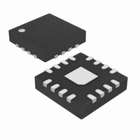
MAX8599ETE+ Maxim Integrated Products, MAX8599ETE+ Datasheet - Page 10

MAX8599ETE+
Manufacturer Part Number
MAX8599ETE+
Description
IC CNTRLR STP DWN LDO 16-TQFN
Manufacturer
Maxim Integrated Products
Datasheet
1.MAX8597ETP.pdf
(24 pages)
Specifications of MAX8599ETE+
Pwm Type
Controller
Number Of Outputs
1
Frequency - Max
1.4MHz
Duty Cycle
99.5%
Voltage - Supply
4.5 V ~ 28 V
Buck
Yes
Boost
No
Flyback
No
Inverting
No
Doubler
No
Divider
No
Cuk
No
Isolated
No
Operating Temperature
-40°C ~ 85°C
Package / Case
16-TQFN Exposed Pad
Frequency-max
1.4MHz
Lead Free Status / RoHS Status
Lead free / RoHS Compliant
Low-Dropout, Wide-Input-Voltage,
Step-Down Controllers
10
MAX8597
10
11
12
13
14
15
16
1
2
3
4
5
6
7
8
9
______________________________________________________________________________________
PIN
MAX8598/
MAX8599
10
11
12
13
14
—
—
1
2
3
4
5
6
7
8
9
REFOUT
NAME
COMP
REFIN
PGND
GND
BST
ILIM
AVL
DH
EN
V+
DL
SS
FB
VL
LX
Filtered VL Input. Connect to VL through a 10Ω resistor. Bypass to GND with a 0.22µF or larger
ceramic capacitor.
External Reference Input. FB tracks the voltage input to REFIN. Connect REFIN to AVL to use
the internal 0.6V reference.
Analog Ground. Connect to the exposed paddle and analog ground plane and then connect to
PGND at the output ground.
Soft-Start Programming Input. Connect a capacitor from SS to GND to set the soft-start time.
See the Selecting the Soft-Start Capacitor section for details.
Feedback Input. Connect to the center tap of an external resistor-divider to set the output
voltage. Regulates to 0.6V for the MAX8598/MAX8599 and MAX8597 when REFIN is connected
to AVL. Regulates to V
Compensation Input. Connect to the required compensation network. See the Compensation
Design section for details.
Enable Input. Drive EN high to enable the IC. Drive low to shut down the IC.
Internal Reference Output. REFOUT regulates to 2.5V and can source up to 1mA. REFOUT
discharges to GND during UVLO.
Input Supply Voltage for Internal VL Regulator. Connect to an input supply in the 4.5V to 28V
range. Bypass to GND with a 1µF or larger ceramic capacitor through a 3Ω resistor.
Internal 5V Linear-Regulator Output. VL provides power for the internal MOSFET gate drivers.
Bypass to PGND with a 1µF or larger ceramic capacitor. VL is always enabled except in
thermal shutdown. See the Internal 5V Linear Regulator section for details.
Low-Side Gate-Driver Output. Connect to the gate of the synchronous rectifier. DL swings from
PGND to VL. DL is held low during shutdown.
Power Ground. Connect to the synchronous rectifier’s source and PGND plane.
Bootstrap Input Supply for the High-Side MOSFET Driver. Connect to the cathode of an external
diode from VL and connect a 0.1µF or larger capacitor from BST to LX.
High-Side Gate-Driver Output. Connect to the gate of the high-side MOSFET. DH swings from
LX to BST. DH is low (connected to LX) during shutdown.
External Inductor Connection. LX is the low supply for the DH gate driver as well as the sense
connection for the current-limit circuitry. Connect LX to the switched side of the inductor as well
as the source of the high-side MOSFET and the drain of the synchronous rectifier.
Current-Limit Sense Input. Connect a resistor from ILIM to the current-sense point to set the
output current limit. See the Setting the Current Limit section for details.
REFIN
(MAX8597) when using an external reference.
FUNCTION
Pin Description


