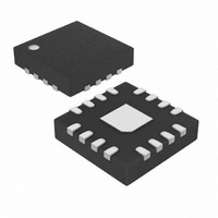
MAX8599ETE+ Maxim Integrated Products, MAX8599ETE+ Datasheet - Page 19

MAX8599ETE+
Manufacturer Part Number
MAX8599ETE+
Description
IC CNTRLR STP DWN LDO 16-TQFN
Manufacturer
Maxim Integrated Products
Datasheet
1.MAX8597ETP.pdf
(24 pages)
Specifications of MAX8599ETE+
Pwm Type
Controller
Number Of Outputs
1
Frequency - Max
1.4MHz
Duty Cycle
99.5%
Voltage - Supply
4.5 V ~ 28 V
Buck
Yes
Boost
No
Flyback
No
Inverting
No
Doubler
No
Divider
No
Cuk
No
Isolated
No
Operating Temperature
-40°C ~ 85°C
Package / Case
16-TQFN Exposed Pad
Frequency-max
1.4MHz
Lead Free Status / RoHS Status
Lead free / RoHS Compliant
Figure 5. Adding RC for More Accurate Sensing
the MOSFET, it is the inductance from the drain to the
source lead.
Alternately, to save board space and cost, the RC net-
works above can be omitted; however, the value of
R
caused by the inductive divider.
An additional switching noise filter may be needed at
ILIM by connecting a capacitor in parallel with R2 (in
the case of R
case of resistor sensing). For the case of R
ing, the value of the capacitor should be:
For the case of resistor sensing:
An external capacitor from SS to GND is charged by an
internal 5µA current source, to the corresponding feed-
back threshold. Therefore, the soft-start time is calculat-
ed as:
For example, 0.033µF from SS to GND yields approxi-
mately a 3.96ms soft-start period.
In the tracking application (see Figure 3), the output
voltage is required to track REFIN during REFIN rise
and fall time. C
than REFIN rise and fall time.
The MAX8597/MAX8598/MAX8599 use a voltage-mode
control scheme that regulates the output voltage by
ILIM
should be raised to account for the voltage step
Selecting the Soft-Start Capacitor
DS(ON)
SS
ILIM
C3 > 15 / (π x f
t
DH
DL
SS
LX
C3 < 25 x 10
______________________________________________________________________________________
must be chosen so that t
= C
sensing) or from ILIM to LX (in the
SS
R2
C3
x V
Compensation Design
FB
-9
S
R
DS(ON)
/ R2
/ 5µA
x R2)
Low-Dropout, Wide-Input-Voltage,
R
C
DS(ON)
ss
is less
sens-
comparing the error-amplifier output (COMP) with a
fixed internal ramp to produce the required duty cycle.
The error amplifier is an operational amplifier with
25MHz bandwidth to provide fast response. The output
lowpass LC filter creates a double pole at the resonant
frequency that introduces a gain drop of 40dB per
decade and a phase shift of 180 degrees per decade.
The error amplifier must compensate for this gain drop
and phase shift to achieve a stable high-bandwidth
closed-loop system. The Type III compensation
scheme (Figure 6) is used to achieve this stability.
The basic regulator loop can be thought of as consist-
ing of a power modulator and an error amplifier. The
power modulator has a DC gain set by V
with a double pole, f
by the output inductor (L), the output capacitor (C
and its equivalent series resistance (R
the equations that define the power modulator:
where C
the total ESR of the output capacitors.
Step-Down Controllers
G
f
f
P LC
Z ESR
MOD DC
_
_
ILIM
O
DH
LX
DL
is the total output capacitance and R
(
=
=
)
C3
2
=
R2
π
2
π
V
P_LC
L C
×
RAMP
1
V
×
R
IN
ESR
, and a single zero, f
1
O
,
×
R
where V
SENSE
C
O
R
C
RAMP
ESR
). Below are
IN
=
1
Z_ESR
V typ
/ V
(
RAMP
ESR
, set
)
O
19
is
),
,


