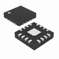
MAX8599ETE+ Maxim Integrated Products, MAX8599ETE+ Datasheet - Page 16

MAX8599ETE+
Manufacturer Part Number
MAX8599ETE+
Description
IC CNTRLR STP DWN LDO 16-TQFN
Manufacturer
Maxim Integrated Products
Datasheet
1.MAX8597ETP.pdf
(24 pages)
Specifications of MAX8599ETE+
Pwm Type
Controller
Number Of Outputs
1
Frequency - Max
1.4MHz
Duty Cycle
99.5%
Voltage - Supply
4.5 V ~ 28 V
Buck
Yes
Boost
No
Flyback
No
Inverting
No
Doubler
No
Divider
No
Cuk
No
Isolated
No
Operating Temperature
-40°C ~ 85°C
Package / Case
16-TQFN Exposed Pad
Frequency-max
1.4MHz
Lead Free Status / RoHS Status
Lead free / RoHS Compliant
Low-Dropout, Wide-Input-Voltage,
Step-Down Controllers
The output voltage is set by a resistor-divider network
from the output to GND with FB at the center tap (R4
and R5 in Figure 4). Select R4 between 5kΩ and 15kΩ
and calculate R5 by:
Using the uncommitted operational amplifier, the
MAX8597 can be configured such that the output volt-
age is adjustable using a voltage source (V
following parameters must be defined before starting
the design:
Select V
put) between 0.05V and 3V and V
than V
(V
V
GND (R6 and R7). Select R7 to be approximately 50kΩ
as a starting point and then calculate R6 as:
Select R4 to be 100kΩ and calculate R5 as:
Select R9 between 5kΩ and 15kΩ, then calculate R8
and R10 as follows:
where V
REFIN connected to AVL).
16
• The minimum desired output voltage, V
• The maximum desired output voltage, V
• The desired input that corresponds to the minimum
• The desired input that corresponds to the maximum
AIN+
R
V
AIN+
8
output voltage, V
output voltage, V
AIN
=
______________________________________________________________________________________
+
[
(
AOUT_MIN
V
) as:
is set using a resistor-divider from REFOUT to
OUT MIN
=
Live Adjustable Output Voltage (see Figure 1)
FB
AOUT
_
(
V
V
R
ADJ MAX
is the feedback regulation voltage (0.6V with
AOUT MAX
−
5
V
R6 = R7 x [(2.5V / V
R5 = R4 x [( V
FB
_
R
(uncommitted operational-amplifier out-
=
)
(
10
×
(
. Calculate the required AIN+ reference
_
V
(
V
OUT MAX
FB
=
(
V
−
_
ADJ_MIN
ADJ_MAX
−
(
AIN
V
V
V
FB
Setting the Output Voltage
AOUT MIN
×
ADJ MIN
(
R
V
×
V
−
8
+
R
ADJ MAX
ADJ MAX
V
×
8
_
FB
_
R
)
+
−
9
) (
[
×
−
(
_
)
V
(
_
+
V
V
FB
OUT
V
OUT MIN
(
OUT MAX
) (
AOUT MIN
V
−
OUT MAX
+
V
_
_
AOUT MIN
V
−
_
/ V
AOUT MAX
V
Fixed Output Voltage
AIN+
−
−
_
AOUT MIN
−
V
_
FB
V
FB
−
FB
V
V
)
FB
)
)
)
AOUT_MAX
_
AIN
) - 1]
×
) - 1]
×
)
R
V
_
×
9
FB
)
(
]
V
+
AOUT MAX
×
OUT_MIN
)
−
OUT_MAX
×
V
R
_
V
AOUT MIN
4
ADJ MIN
ADJ
−
V
_
FB
higher
_
). The
)
]
×
R
9
)
Additionally, to minimize error, R6 and R7 should be
chosen such that:
There are several parameters that must be examined
when determining which inductor is to be used: input
voltage, output voltage, load current, switching fre-
quency, and LIR. LIR is the ratio of inductor current rip-
ple to DC load current. A higher LIR value allows for a
smaller inductor but results in higher losses and higher
output ripple. A good compromise between size and
efficiency is a 30% LIR. Once all the parameters are
chosen, the inductor value is determined as follows:
where f
value close to the calculated value. The exact inductor
value is not critical and can be adjusted in order to
make trade-offs among size, cost, and efficiency.
Lower inductor values minimize size and cost, but also
increase the output ripple and reduce the efficiency
due to higher peak currents. On the other hand, higher
inductor values increase efficiency, but eventually
resistive losses due to extra turns of wire exceed the
benefit gained from lower AC current levels. Find a low-
loss inductor having the lowest possible DC resistance
that fits the allotted dimensions. Ferrite cores are often
the best choice, although powdered iron is inexpensive
and can work well up to 300kHz. The chosen inductor’s
saturation current rating must exceed the peak inductor
current determined as:
The input filter capacitor reduces peak currents drawn
from the power source and reduces noise and voltage
ripple on the input caused by the circuit’s switching.
The input capacitor must meet the ripple current
requirement (I
defined by the following equation:
I
I
RMS
S
PEAK
L
is the switching frequency. Choose a standard
=
=
=
V
RMS
IN
I
LOAD
I
LOAD MAX
x f
R
R
) imposed by the switching currents
V
6
6
OUT
S
(
×
+
×
x I
R
R
7
x V
7
LOAD MAX
)
V
=
+
OUT
(
R
R
IN
V
⎛
⎜
⎝
4
4
IN
(
LIR
Inductor Selection
−
2
×
×
+
V
OUT
⎞
⎟ ×
⎠
Input Capacitor
(
R
R
)
V
5
5
IN
x LIR
)
I
−
LOAD MAX
V
OUT
(
)
)


