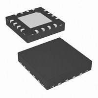
ISL8104IRZ Intersil, ISL8104IRZ Datasheet - Page 12

ISL8104IRZ
Manufacturer Part Number
ISL8104IRZ
Description
IC PWM CTRLR BUCK 1PHASE 16-QFN
Manufacturer
Intersil
Datasheet
1.ISL8104IBZ.pdf
(14 pages)
Specifications of ISL8104IRZ
Pwm Type
Voltage Mode
Number Of Outputs
1
Frequency - Max
1.5MHz
Duty Cycle
100%
Voltage - Supply
7.6 V ~ 15.4 V
Buck
Yes
Boost
No
Flyback
No
Inverting
No
Doubler
No
Divider
No
Cuk
No
Isolated
No
Operating Temperature
-40°C ~ 85°C
Package / Case
16-VQFN Exposed Pad, 16-HVQFN, 16-SQFN, 16-DHVQFN
Frequency-max
1.5MHz
Input Voltage
15.4V
Output Voltage
5V
Frequency
1.5MHz
Supply Voltage Range
8V To 14V
Digital Ic Case Style
QFN
No. Of Pins
16
Operating Temperature Range
-40°C To +85°C
Filter Terminals
SMD
Rohs Compliant
Yes
Controller Type
PWM
Lead Free Status / RoHS Status
Lead free / RoHS Compliant
Standard-gate MOSFETs are normally recommended for
use with the ISL8104. However, logic-level gate MOSFETs
can be used under special circumstances. The input voltage,
top-side gate drive level, and the MOSFETs absolute gate-
to-source voltage rating determine whether logic-level
MOSFETs are appropriate.
Figure 9 shows the top-side gate drive (BOOT pin) supplied
by a bootstrap circuit from +14V. The boot capacitor, C
develops a floating supply voltage referenced to the LX pin.
This supply is refreshed each cycle to a voltage of +14V less
the boot diode drop (V
turns on. A MOSFET can only be used for Q
MOSFETs absolute gate-to-source voltage rating exceeds
the maximum voltage applied to +14V. For Q
MOSFET can be used if its absolute gate-to-source voltage
rating also exceeds the maximum voltage applied to +14V.
Figure 10 shows the top-side gate drive supplied by a direct
connection to +14V. This option should only be used in
converter systems where the main input voltage is +5VDC or
less. The peak top-side gate-to-source voltage is
approximately +14V less the input supply. For +5V main
power and +14VDC for the bias, the gate-to-source voltage
of Q
and a logic-level MOSFET can be used for Q
gate-to-source voltage rating exceeds the maximum voltage
applied to PVCC. This method reduces the number of
required external components, but does not provide for
immunity to phase node ringing during turn on and may
result in lower system efficiency.
Schottky Selection
Rectifier D2 is a clamp that catches the negative inductor
swing during the dead time between turning off the bottomside
MOSFET and turning on the top-side MOSFET. The diode
must be a Schottky type to prevent the lossy parasitic
MOSFET body diode from conducting. It is acceptable to omit
the diode and let the body diode of the bottom-side MOSFET
clamp the negative inductor swing, but efficiency could slightly
decrease as a result. The diode's rated reverse breakdown
voltage must be greater than the maximum input voltage.
1
is 9V. A logic-level MOSFET is a good choice for Q
D
) when the bottom-side MOSFET, Q
12
1
2
2
, a logic-level
if the
if its absolute
BOOT
1
2
ISL8104
FIGURE 10. TOP-SIDE GATE DRIVE - DIRECT V
FIGURE 9. TOP-SIDE GATE DRIVE - BOOTSTRAP OPTION
+
+
-
-
ISL8104
ISL8104
+14V
+14V
OPTION
+
GND
D
GND
V
BOOT
D
BOOT
TGATE
BGATE
PGND
BOOT
TGATE
BGATE
PGND
PVCC
PVCC
LX
-
+14V
+14V
C
BOOT
Q1
Q2
Q1
Q2
+1.2V TO +14V
+5V OR LESS
D2
D2
V
NOTE:
V
NOTE:
NOTE:
V
NOTE:
V
G-S
G-S
G-S
G-S
CC
≈
≈
≈
≈
DRIVE
March 7, 2008
V
V
PVCC
PVCC
CC
CC
FN9257.2
- 5V
- V
D


