ISL8106CRZ Intersil, ISL8106CRZ Datasheet - Page 11
ISL8106CRZ
Manufacturer Part Number
ISL8106CRZ
Description
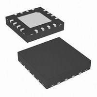
IC PWM CTRLR SGL PHASE 16-QFN
Manufacturer
Intersil
Datasheet
1.ISL8106CRZ.pdf
(15 pages)
Specifications of ISL8106CRZ
Pwm Type
Voltage Mode
Number Of Outputs
1
Frequency - Max
600kHz
Voltage - Supply
7 V ~ 25 V
Buck
Yes
Boost
No
Flyback
No
Inverting
No
Doubler
No
Divider
No
Cuk
No
Isolated
No
Operating Temperature
0°C ~ 70°C
Package / Case
16-VQFN Exposed Pad, 16-HVQFN, 16-SQFN, 16-DHVQFN
Frequency-max
600kHz
Lead Free Status / RoHS Status
Lead free / RoHS Compliant
Duty Cycle
-
Available stocks
Company
Part Number
Manufacturer
Quantity
Price
Company:

Part Number:
ISL8106CRZ
Manufacturer:
Intersil
Quantity:
500


levels. Keep the metal runs from the LX terminals to the
output inductor short. The power plane should support the
input power and output power nodes. Use copper filled
polygons on the top and bottom circuit layers for the LX
nodes. Use the remaining printed circuit layers for small
signal wiring.
Locate the ISL8106 within 2 to 3 inches of the MOSFETs, Q1
and Q2 (1 inch or less for 500kHz or higher operation). The
circuit traces for the MOSFETs’ gate and source connections
from the ISL8106 must be sized to handle up to 4A peak
current. Provide local V
GND pins. Locate the capacitor, C
to the BOOT pin and the phase node.
Programming the Output Voltage
When the converter is in regulation there will be 600mV from
the FB pin to the GND pin. Connect a two-resistor voltage
divider across the VO pin and the GND pin with the output
node connected to the FB pin. Scale the voltage-divider
network such that the FB pin is 600mV with respect to the
GND pin when the converter is regulating at the desired
output voltage.
Programming the output voltage can be written as:
Where:
Calculating the value of R
Programming the PWM Switching Frequency
The PWM switching frequency F
resistor R
GND pin. Programming the approximate PWM switching
frequency can be written as:
Estimating the value of R
V
F
R
R
OSC
REF
FSET
BOTTOM
- V
- V
- R
- R
FB pin.
from the FB pin to the VO pin. It is usually chosen to set
the gain of the control-loop error amplifier. It follows that
R
selected value of R
connects from the FB pin to the GND pin.
OUT
REF
TOP
BOTTOM
BOTTOM
=
=
=
V
-------------------------------------------------------------- -
60 R
FSET
------------------------------------------------------- -
60 F
OUT
is the voltage that the converter regulates to at the
is the voltage-programming resistor that connects
is the desired output voltage of the converter.
=
•
•
------------------------------------ -
V
V
FSET
•
OSC
OUT
-------------------------------------------------- -
R
REF
will be calculated based upon the already
is the voltage-programming resistor that
that is connected from the FSET pin to the
TOP
1
1
R
•
•
•
–
[
[
R
BOTTOM
1
1
V
+
TOP
×10
REF
×
R
CC
TOP.
10
BOTTOM
FSET
–
BOTTOM
12
–
decoupling between VCC and
12
]
11
]
can now be written as:
OSC
BOOT
can now be written as:
is programmed by the
as close as practical
(EQ. 6)
(EQ. 5)
(EQ. 7)
(EQ. 8)
ISL8106
Where:
Selection of the LC Output Filter
The duty cycle of a buck converter is ideally a function of the
input voltage and the output voltage. This relationship can be
written as:
Where:
The output inductor peak-to-peak ripple current can be
written as:
Where:
A typical step-down DC/DC converter will have an I
20% to 40% of the nominal DC output load current. The
value of I
MOSFET switching loss, inductor core loss, and the
resistance the inductor winding, DCR. The DC copper loss of
the inductor can be estimated by:
The inductor copper loss can be significant in the total
system power loss. Attention has to be given to the DCR
selection. Another factor to consider when choosing the
inductor is its saturation characteristics at elevated
temperature. A saturated inductor could cause destruction of
circuit components, as well as nuisance OCP faults.
A DC/DC buck regulator must have output capacitance C
into which ripple current I
corresponding ripple voltage V
sum of the voltage drop across the capacitor ESR and of the
voltage change stemming from charge moved in and out of
the capacitor. These two voltages can be written as:
and
If the output of the converter has to support a load with high
pulsating current, several capacitors will need to be
D V
I
P
ΔV
PP
COPPER
ΔV
(
- F
- R
- 60 x [1 x 10
- D is the PWM duty cycle.
- V
- V
- I
- F
- L
ESR
IN
=
C
PP
O
OSC
OSC
FSET
)
IN
OUT
V
---------------------------------------------------- -
=
=
OUT
is the nominal value of the output inductor.
=
is the peak-to-peak output inductor ripple current.
is the input voltage to be converted.
---------------------------------- -
8 C
PP
V
--------------- -
I
•
=
PP
F
is the PWM switching frequency.
V
is the regulated output voltage of the converter.
is the PWM switching frequency.
OUT
is the F
•
OSC
IN
is selected based upon several criteria such as
O
[
[
I
•
I
PP
1 D V
LOAD
E
•
F
–
SR
-12
OSC
•
L
(
O
] is a constant.
OSC
]
2
IN
•
DCR
)
]
programming resistor.
PP
can flow. Current I
PP
across C
O,
which is the
PP
November 10, 2006
develops a
PP
(EQ. 13)
(EQ. 10)
(EQ. 12)
(EQ. 11)
FN9283.1
(EQ. 9)
of
O
Related parts for ISL8106CRZ
Image
Part Number
Description
Manufacturer
Datasheet
Request
R

Part Number:
Description:
Single-Phase PWM Controller
Manufacturer:
Intersil Corporation
Datasheet:
Part Number:
Description:
Intersil Corporation [CMOS Serial Controller Interface]
Manufacturer:
Intersil Corporation
Datasheet:
Part Number:
Description:
Manufacturer:
Intersil Corporation
Datasheet:
Part Number:
Description:
357-036-542-201 CARDEDGE 36POS DL .156 BLK LOPRO
Manufacturer:
Intersil Corporation
Datasheet:
Part Number:
Description:
1024-Word x 4-Bit LSI Static RAM
Manufacturer:
Intersil Corporation
Datasheet:
Part Number:
Description:
General Purpose NPN Transistor Arrays FN341.4
Manufacturer:
Intersil Corporation
Datasheet:
Part Number:
Description:
CMOS 16-Bit Microprocessor
Manufacturer:
Intersil Corporation
Datasheet:
Part Number:
Description:
Manufacturer:
Intersil Corporation
Datasheet:
Part Number:
Description:
Manufacturer:
Intersil Corporation
Datasheet:
Part Number:
Description:
Manufacturer:
Intersil Corporation
Datasheet:
Part Number:
Description:
Manufacturer:
Intersil Corporation
Datasheet:
Part Number:
Description:
CMOS 6-Bit Latch and Decoder Memory Interfaces
Manufacturer:
Intersil Corporation
Datasheet:
Part Number:
Description:
CA3046General Purpose NPN Transistor Arrays
Manufacturer:
Intersil Corporation
Datasheet:
Part Number:
Description:
Manufacturer:
Intersil Corporation
Datasheet:
Part Number:
Description:
TR909 DLC/FLC SLIC with Low Power Standby
Manufacturer:
Intersil Corporation
Datasheet: