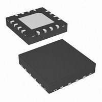
ISL8106CRZ Intersil, ISL8106CRZ Datasheet - Page 13

ISL8106CRZ
Manufacturer Part Number
ISL8106CRZ
Description
IC PWM CTRLR SGL PHASE 16-QFN
Manufacturer
Intersil
Datasheet
1.ISL8106CRZ.pdf
(15 pages)
Specifications of ISL8106CRZ
Pwm Type
Voltage Mode
Number Of Outputs
1
Frequency - Max
600kHz
Voltage - Supply
7 V ~ 25 V
Buck
Yes
Boost
No
Flyback
No
Inverting
No
Doubler
No
Divider
No
Cuk
No
Isolated
No
Operating Temperature
0°C ~ 70°C
Package / Case
16-VQFN Exposed Pad, 16-HVQFN, 16-SQFN, 16-DHVQFN
Frequency-max
600kHz
Lead Free Status / RoHS Status
Lead free / RoHS Compliant
Duty Cycle
-
Available stocks
Company
Part Number
Manufacturer
Quantity
Price
Company:
Part Number:
ISL8106CRZ
Manufacturer:
Intersil
Quantity:
500
P
For the top-side MOSFET, its switching loss can be written
as:
The peak and valley current of the inductor can be obtained
based on the inductor peak-to-peak current and the load
current. The turn-on and turn-off time can be estimated with
the given gate driver parameters in the Electrical
Specification Table.
Selecting The Bootstrap Capacitor
The selection of the bootstrap capacitor can be written as:
Where:
As an example, suppose the top-side MOSFET has a total
gate charge Q
200mV. The calculated bootstrap capacitance is 0.125µF;
select at least the first standard component value of greater
capacitance than calculated, that being 0.15µF. Use an X7R
or X5R ceramic capacitor.
Compensating the Converter
The LC output filter has a double pole at its resonant frequency
that causes the phase to abruptly roll downward. The R
modulator used in the ISL8106 makes the LC output filter
resemble a first order system in which the closed loop stability
can be achieved with a Type II compensation network.
C
SWTS
BOOT
- Q
- ΔV
side MOSFET
the boot capacitor each time the MOSFET is switched on
g
(
FIGURE 6. SYSTEM CONTROL BLOCK DIAGRAM
V
BOOT
is the total gate charge required to switch the top-
=
IN
----------------------- -
ΔV
)
=
, is the maximum allowed voltage decay across
Q
BOOT
R
G
V
------------------------------------------------------------ -
g
TOP
, of 25nC at V
IN
•
I
VAL
•
2
T
V
ON
REF
FB
13
•
GS
F
C
OSC
COMP2
AMPLIFIER
= 5V, and a ΔV
−
+
ERROR
+
V
-------------------------------------------------------------------- -
C
COMP1
IN
•
I
PEAK
R
COMP
COMP
•
BOOT
2
T
OFF
(EQ. 18)
(EQ. 17)
3
•
of
F
OSC
ISL8106
Figure 7 highlights the voltage-mode control loop for a
synchronous-rectified buck converter. The output voltage is
regulated to the reference voltage level. The error amplifier
output is compared with the oscillator triangle wave to
provide a pulse-width modulated wave with an amplitude of
V
output filter. The output filter capacitor bank’s equivalent
series resistance is represented by the series resistor ESR.
IN
at the LX node. The PWM wave is smoothed by the
ISL8106
R
Gate Drivers
COMP
FIGURE 7. COMPENSATION REFERENCE CIRCUIT
3
Modulator
R
GND
COMP
REF
EA
C
BGATE
TGATE
+
COMP1
-
FSET
VO
VIN
FB
LX
C
COMP2
R
FSET
Q
Q
R
TOP_SIDE
BOTTOM_SIDE
BOTTOM
L
R
OUT
VIN
TOP
November 10, 2006
C
DCR
ESR
C
OUT
FSET
FN9283.1


