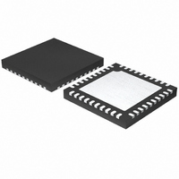
ISL6308IRZ-T Intersil, ISL6308IRZ-T Datasheet - Page 12

ISL6308IRZ-T
Manufacturer Part Number
ISL6308IRZ-T
Description
IC CTRLR PWM 3PHASE BUCK 40-QFN
Manufacturer
Intersil
Datasheet
1.ISL6308CRZ.pdf
(28 pages)
Specifications of ISL6308IRZ-T
Pwm Type
Voltage Mode
Number Of Outputs
1
Frequency - Max
275kHz
Duty Cycle
66.6%
Voltage - Supply
4.75 V ~ 5.25 V
Buck
Yes
Boost
No
Flyback
No
Inverting
No
Doubler
No
Divider
No
Cuk
No
Isolated
No
Operating Temperature
-40°C ~ 85°C
Package / Case
40-VFQFN, 40-VFQFPN
Frequency-max
275kHz
Lead Free Status / RoHS Status
Lead free / RoHS Compliant
to VSEN pin to set the output voltage level as shown in
Figure 6. This method is good for generating voltages up to
2.3V (with the REF voltage set to 1.5V).
For this case, the output voltage can be obtained as follows:
V
It is recommended to choose resistor values of less than
500Ω for R
voltage DC accuracy.
Voltage Regulation
In order to regulate the output voltage to a specified level, the
ISL6308 uses the integrating compensation network shown in
Figure 6. This compensation network insures that the steady
state error in the output voltage is limited only to the error in
the reference voltage (output of the DAC or the external
voltage reference) and offset errors in the OFS current
source, remote sense and error amplifiers. Intersil specifies
the guaranteed tolerance of the ISL6308 to include the
combined tolerances of each of these elements, except when
an external reference or voltage divider is used, then the
tolerances of these components has to be taken into account.
The ISL6308 incorporates an internal differential remote
sense amplifier in the feedback path. The amplifier removes
the voltage error encountered when measuring the output
voltage relative to the controller ground reference point,
resulting in a more accurate means of sensing output voltage.
Connect the microprocessor sense pins to the non-inverting
input, VSEN, and inverting input, RGND, of the remote-sense
amplifier. The droop voltage, VDROOP, also feeds into the
remote-sense amplifier. The remote-sense output, VDIFF, is
therefore equal to the sum of the output voltage, VOUT, and
the droop voltage. VDIFF is connected to the inverting input of
the error amplifier through an external resistor.
The output of the error amplifier, V
sawtooth waveform to generate the PWM signals. The PWM
signals control the timing of the Internal MOSFET drivers
and regulate the converter output so that the voltage at FB is
equal to the voltage at REF. This will regulate the output
voltage to be equal to Equation 5. The internal and external
OUT
TABLE 1. ISL6308 DAC VOLTAGE SELECTION TABLE
=
REF1
V
0
0
1
1
REF
S1
and R
⋅
(
--------------------------------- -
R
S1
R
P1
+
P1
R
resistors in order to get better output
P1
)
+ −
REF0
V
12
0
1
0
1
OFS
COMP
–
V
DROOP
, is compared to the
VDA (V)
0.600
0.900
1.200
1.500
(EQ. 4)
ISL6308
circuitry that controls voltage regulation is illustrated in
Figure 6.
V
OUT
R
FIGURE 6. OUTPUT VOLTAGE AND LOAD-LINE
1
V
C
=
DROOP
EXTERNAL CIRCUIT
SUM
+
-
V
V
V
OUT
REF
OFS
R
+
+
-
-
2
REGULATION WITH OFFSET ADJUSTMENT
±
R
C
S1
V
1
OFST
C
DROOP
REF
ICOMP
COMP
VDIFF
VSEN
RGND
ISUM
IREF
REF
R
DAC
FB
P1
–
V
DROOP
ISL6308 INTERNAL CIRCUIT
I
OFS
VID DAC
+
-
ERROR AMPLIFIER
+
+
-
-
ISENSE
AMP
REMOTE-SENSE
DIFFERENTIAL
AMPLIFIER
+
-
September 30, 2008
V
COMP
FN9208.4
(EQ. 5)


