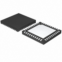
ISL6308IRZ-T Intersil, ISL6308IRZ-T Datasheet - Page 14

ISL6308IRZ-T
Manufacturer Part Number
ISL6308IRZ-T
Description
IC CTRLR PWM 3PHASE BUCK 40-QFN
Manufacturer
Intersil
Datasheet
1.ISL6308CRZ.pdf
(28 pages)
Specifications of ISL6308IRZ-T
Pwm Type
Voltage Mode
Number Of Outputs
1
Frequency - Max
275kHz
Duty Cycle
66.6%
Voltage - Supply
4.75 V ~ 5.25 V
Buck
Yes
Boost
No
Flyback
No
Inverting
No
Doubler
No
Divider
No
Cuk
No
Isolated
No
Operating Temperature
-40°C ~ 85°C
Package / Case
40-VFQFN, 40-VFQFPN
Frequency-max
275kHz
Lead Free Status / RoHS Status
Lead free / RoHS Compliant
Once the desired output offset voltage has been determined,
use the following formulas to set R
For Positive Offset (connect R
For Negative Offset (connect R
R
R
V
R
OFS
OFS
V
R
OFS
OFS
FIGURE 9. NEGATIVE OFFSET OUTPUT VOLTAGE
+
-
FIGURE 8. POSITIVE OFFSET OUTPUT VOLTAGE
OFS
OFS
+
VDIFF
-
VDIFF
VCC
=
=
GND
R
I
I
OFS
--------------------------
V
--------------------------
V
OFS
R
1
OFS
0.5 R
1.5 R
OFFSET
OFFSET
1
OFS
FB
FB
⋅
⋅
PROGRAMMING
PROGRAMMING
1
1
ISL6308
ISL6308
VREF
VREF
14
OFS
OFS
OFS
to GND):
to VCC):
:
E/A
GND
E/A
GND
+
-
+
-
0.5V
0.5V
VCC
VCC
(EQ. 10)
(EQ. 9)
+
-
+
-
1.5V
1.5V
ISL6308
Advanced Adaptive Zero Shoot-Through Deadtime
Control (Patent Pending)
The integrated drivers incorporate a unique adaptive
deadtime control technique to minimize deadtime, resulting
in high efficiency from the reduced freewheeling time of the
lower MOSFET body-diode conduction, and to prevent the
upper and lower MOSFETs from conducting simultaneously.
This is accomplished by ensuring either rising gate turns on
its MOSFET with minimum and sufficient delay after the
other has turned off.
During turn-off of the lower MOSFET, the PHASE voltage is
monitored until it reaches a -0.3V/+0.8V trip point for a
forward/reverse current, at which time the UGATE is
released to rise. An auto-zero comparator is used to correct
the r
detection of the -0.3V phase level during r
period. In the case of zero current, the UGATE is released
after 35ns delay of the LGATE dropping below 0.5V. During
the phase detection, the disturbance of LGATE falling
transition on the PHASE node is blanked out to prevent
falsely tripping. Once the PHASE is high, the advanced
adaptive shoot-through circuitry monitors the PHASE and
UGATE voltages during a PWM falling edge and the
subsequent UGATE turn-off. If either the UGATE falls to less
than 1.75V above the PHASE or the PHASE falls to less than
+0.8V, the LGATE is released to turn on.
Internal Bootstrap Device
All three integrated drivers feature an internal bootstrap
Schottky diode. Simply adding an external capacitor across
the BOOT and PHASE pins completes the bootstrap circuit.
The bootstrap function is also designed to prevent the
bootstrap capacitor from overcharging due to the large
negative swing at the PHASE node. This reduces voltage
stress on the boot to phase pins.
The bootstrap capacitor must have a maximum voltage
rating above PVCC + 5V and its capacitance value can be
chosen from Equation 11:
where Q
at V
control MOSFETs. The ΔV
allowable droop in the rail of the upper gate drive. Figure 10
shows the boot capacitor ripple voltage as a function of boot
capacitor value and total upper MOSFET gate charge.
C
Q
BOOT_CAP
GATE
GS1
DS(ON)
=
G1
gate-source voltage and N
Q
-------------------------------- - N
G1
is the amount of gate charge per upper MOSFET
drop in the phase voltage preventing false
≥
V
•
GS1
------------------------------------- -
ΔV
PVCC
BOOT_CAP
Q
GATE
•
Q1
BOOT_CAP
Q1
term is defined as the
is the number of
DS(ON)
September 30, 2008
conduction
(EQ. 11)
FN9208.4


