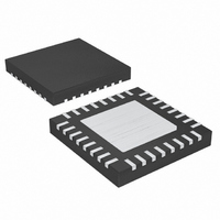
MAX17528GTJ+ Maxim Integrated Products, MAX17528GTJ+ Datasheet - Page 25

MAX17528GTJ+
Manufacturer Part Number
MAX17528GTJ+
Description
IC PWM CTRLR STP-DWN 32TQFN-EP
Manufacturer
Maxim Integrated Products
Series
Quick-PWM™r
Datasheet
1.MAX17528GTJ.pdf
(41 pages)
Specifications of MAX17528GTJ+
Applications
Controller, Intel IMVP-6.5™ GMCH
Voltage - Input
4.5 ~ 5.5 V
Number Of Outputs
1
Voltage - Output
0.01 ~ 1.5 V
Operating Temperature
-40°C ~ 105°C
Mounting Type
Surface Mount
Package / Case
32-TQFN Exposed Pad
Lead Free Status / RoHS Status
Lead free / RoHS Compliant
The nominal no-load output voltage (V
defined by the VID-selected DAC voltage (see Table 2)
plus the remote ground-sense adjustment (V
defined in the following equation:
where V
IMVP-6.5 (CLKEN pullup to 3.3V with 1.9kΩ) applica-
tions slew the target voltage from ground to the preset
1.1V boot voltage and GMCH (CLKEN = GND) applica-
tions slew the target voltage directly to the VID-selected
DAC target.
The MAX17528 includes a transconductance amplifier
for adding gain to the voltage-positioning sense path.
The amplifier’s input is generated by the differential
current-sense inputs that sense the inductor current by
measuring the voltage across either current-sense
resistors or the inductor’s DCR. The amplifier’s output
connects directly to the regulator’s voltage-positioned
feedback input (FB), so the resistance between FB and
the output-voltage sense point determines the voltage-
positioning gain:
where the target voltage (V
the selected VID code (Table 3 for IMVP6 or Table 4 for
GMCH), and the FB amplifier’s output current (I
determined by the sum of the current-sense voltages:
where G
Electrical Characteristics table.
The MAX17528 includes differential, remote-sense
inputs to eliminate the effects of voltage drops along the
PCB traces and through the processor’s power pins.
The feedback-sense node connects to the voltage-posi-
tioning resistor (R
DAC
m(FB)
V
TARGET
is the selected VID voltage. On startup,
I
V
FB
is typically 600µS as defined in the
OUT
FB
=
______________________________________________________________________________________
G
). The ground-sense (GNDS) input
=
m FB
=
V
(
V
TARGET
Voltage-Positioning Amplifier
FB
)
(
TARGET
=
V
Differential Remote Sense
CSP
V
DAC
−
−
(Steady-State Droop)
R I
V
+
FB FB
= V
CSN
V
Intel IMVP-6.5/GMCH Controllers
GNDS
FB
)
) is defined by
Feedback
TARGET
GNDS
FB
) as
) is
) is
connects to an amplifier that adds an offset directly to
the feedback voltage, effectively adjusting the output
voltage to counteract the voltage drop in the ground
path. Connect the voltage-positioning resistor (R
ground-sense (GNDS) input directly to the processor’s
remote-sense outputs as shown in Figures 1 and 2.
An integrator amplifier forces the DC average of the FB
voltage to equal the target voltage. This transconduc-
tance amplifier integrates the feedback voltage and
provides a fine adjustment to the regulation voltage
(Figure 3), allowing accurate DC output-voltage regula-
tion regardless of the output ripple voltage. The integra-
tor amplifier has the ability to shift the output voltage by
±50mV (typ). The integration time constant can be set
easily with an external compensation capacitor
between CCV and analog ground, with the minimum
recommended CCV capacitor value determined by:
where G
transconductance and f
set by the R
The MAX17528 disables the integrator by connecting
the amplifier inputs together at the beginning of all
downward VID transitions done in pulse-skipping mode
(SKIP = high). The integrator remains disabled until
20µs after the transition is completed (the internal tar-
get settles) and the output is in regulation (edge detect-
ed on the error comparator).
The digital-to-analog converter (DAC) programs the
output voltage using the D0–D6 inputs. D0–D6 are low-
voltage (1.0V) logic inputs designed to interface direct-
ly with the CPU. Do not leave D0–D6 unconnected.
Changing D0–D6 initiates a transition to a new output-
voltage level. Change D0–D6 together, avoiding
greater than 20ns skew between bits. Otherwise, incor-
rect DAC readings can cause a partial transition to the
wrong voltage level followed by the intended transition
to the correct voltage level, lengthening the overall tran-
sition time. The available DAC codes and resulting out-
put voltages are compatible with the Intel IMVP-6.5/
GMCH specifications (Table 2).
1-Phase Quick-PWM
m(CCV)
TON
C
CCV
resistance.
= 320µS (max) is the integrator’s
>> G
m(CCV)
SW
is the switching frequency
DAC Inputs (D0–D6)
/(16π x f
Integrator Amplifier
SW
)
FB
) and
25


