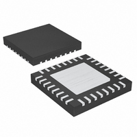
MAX17528GTJ+ Maxim Integrated Products, MAX17528GTJ+ Datasheet - Page 39

MAX17528GTJ+
Manufacturer Part Number
MAX17528GTJ+
Description
IC PWM CTRLR STP-DWN 32TQFN-EP
Manufacturer
Maxim Integrated Products
Series
Quick-PWM™r
Datasheet
1.MAX17528GTJ.pdf
(41 pages)
Specifications of MAX17528GTJ+
Applications
Controller, Intel IMVP-6.5™ GMCH
Voltage - Input
4.5 ~ 5.5 V
Number Of Outputs
1
Voltage - Output
0.01 ~ 1.5 V
Operating Temperature
-40°C ~ 105°C
Mounting Type
Surface Mount
Package / Case
32-TQFN Exposed Pad
Lead Free Status / RoHS Status
Lead free / RoHS Compliant
Worst-case conduction losses occur at the duty factor
extremes. For the high-side MOSFET (N
case power dissipation due to resistance occurs at the
minimum input voltage:
Generally, a small high-side MOSFET is desired to
reduce switching losses at high input voltages.
However, the R
power dissipation often limits how small the MOSFET
can be. Again, the optimum occurs when the switching
losses equal the conduction (R
side switching losses do not usually become an issue
until the input is greater than approximately 15V.
Calculating the power dissipation in high-side MOSFET
(N
must allow for difficult quantifying factors that influence
the turn-on and turn-off times. These factors include the
internal gate resistance, gate charge, threshold volt-
age, source inductance, and PCB layout characteris-
tics. The following switching-loss calculation provides
only a very rough estimate and is no substitute for
breadboard evaluation, preferably including verification
using a thermocouple mounted on N
where C
Q
and I
(2.2A typ).
Switching losses in the high-side MOSFET can become
an insidious heat problem when maximum AC adapter
voltages are applied, due to the squared term in the
C x V
MOSFET chosen for adequate R
voltages becomes extraordinarily hot when biased from
V
lower parasitic capacitance.
For the low-side MOSFET (N
dissipation always occurs at maximum input voltage:
The worst case for MOSFET power dissipation occurs
under heavy overloads that are greater than
PD NHSwitching
IN(MAX)
G(SW)
H
(
) due to switching losses is complicated since it
PD NL
GATE
IN
PD NH
(
2
is the charge needed to turn on the N
OSS
(
x f
, consider choosing another MOSFET with
Re
is the peak gate-drive source/sink current
SW
Re
sistive
is the N
)
sistive
switching-loss equation. If the high-side
DS(ON)
=
V
______________________________________________________________________________________
IN MAX LOAD SW
)
=
(
MOSFET Power Dissipation
⎡
⎢
⎢
⎣
)
H
1
=
−
required to stay within package
)
MOSFET’s output capacitance,
⎛
⎜
⎝
I
⎛
⎜
⎝
V
V
OUT
V
IN MAX
V
IN
OUT
(
f
L
), the worst-case power
⎞
⎟
⎠
⎛
⎜
⎝
(
DS(ON)
)
I
Q
LOAD
DS(ON)
I
⎞
⎟
⎠
GATE
G SW
⎤
⎥
⎥
⎦
(
(
H
I
LOAD
Intel IMVP-6.5/GMCH Controllers
:
)
)
2
) losses. High-
⎞
⎟ +
⎠
R
at low battery
H
)
DS ON
C
2
), the worst-
R
OSS IN SW
H
(
DS ON
MOSFET,
V
(
2
)
2
f
)
I
the current limit and cause the fault latch to trip. To pro-
tect against this possibility, you can “over design” the
circuit to tolerate:
where I
allowed by the current-limit circuit, including threshold
tolerance and on-resistance variation. The MOSFETs
must have a good-size heatsink to handle the overload
power dissipation.
Choose a Schottky diode (D
low enough to prevent the low-side MOSFET body
diode from turning on during the dead time. Select a
diode that can handle the load current during the dead
times. This diode is optional and can be removed if effi-
ciency is not critical.
The boost capacitors (C
enough to handle the gate-charging requirements of
the high-side MOSFETs. Typically, 0.1µF ceramic
capacitors work well for low-power applications driving
medium-sized MOSFETs. However, high-current appli-
cations driving large, high-side MOSFETs require boost
capacitors larger than 0.1µF. For these applications,
select the boost capacitors to avoid discharging the
capacitor more than 200mV while charging the high-
side MOSFETs’ gates:
where N is the number of high-side MOSFETs used for
one regulator, and Q
in the MOSFET’s data sheet. For example, assume (2)
IRF7811W n-channel MOSFETs are used on the high
side. According to the manufacturer’s data sheet, a sin-
gle IRF7811W has a maximum gate charge of 24nC
(V
boost capacitance would be:
Selecting the closest standard value, this example
requires a 0.22µF ceramic capacitor.
LOAD(MAX)
I
LOAD
GS
= 5V). Using the above equation, the required
1-Phase Quick-PWM
=
VALLEY(MAX)
⎛
⎜
⎝
I
VALLEY MAX
, but are not quite high enough to exceed
C
BST
(
C
BST
=
GATE
is the maximum valley current
)
2 24
200
+
=
×
BST
N Q
∆
is the gate charge specified
I
mV
INDUCTOR
×
200
nC
) must be selected large
L
) with a forward voltage
GATE
2
mV
=
Boost Capacitors
0 24
.
⎞
⎟ =
⎠
µF
I
VALLEY MAX
(
39
)


