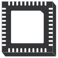
L6756D STMicroelectronics, L6756D Datasheet - Page 27

L6756D
Manufacturer Part Number
L6756D
Description
IC CTLR 2/3/4PH BUCK 40-VFQFPN
Manufacturer
STMicroelectronics
Datasheet
1.L6756DTR.pdf
(36 pages)
Specifications of L6756D
Applications
Controller, Intel VR10, VR11, VR11.1
Voltage - Input
12V
Number Of Outputs
4
Voltage - Output
0.3 ~ 1.6 V
Operating Temperature
0°C ~ 70°C
Mounting Type
Surface Mount
Package / Case
40-VFQFN, 40-VFQFPN
Output Voltage
3 V
Input Voltage
- 0.3 V to + 15 V
Switching Frequency
185 KHz to 215 KHz
Operating Temperature Range
- 40 C to + 150 C
Mounting Style
SMD/SMT
Lead Free Status / RoHS Status
Lead free / RoHS Compliant
Available stocks
Company
Part Number
Manufacturer
Quantity
Price
L6756D
6.3
6.4
Note:
VR_RDY
It is an open-drain signal set free after the soft-start sequence has finished.
Over current
The over current threshold has to be programmed to a safe value, in order to be sure that
the system doesn't enter OC during normal operation. This value must take into
consideration also the extra current needed during the DVID transition (I
process spread and temperature variations of the sensing elements (inductor DCR).
Moreover, since also the internal threshold spreads, the design has to consider the
minimum/maximum value of the thresholds.
L6756D monitors the average current and allows to set the OC threshold by programming
R
copy of the DROOP current is sourced from the ILIM pin. By connecting a resistor R
SGND, a load indicator with 1.7 V (V
when the voltage present at the ILIM pin crosses 1.7 V, the device detects an OC and
immediately latches with all the mosfets OFF (HiZ).
Typical design flow is the following:
OC intervention can be delayed by adding a capacitor in parallel to the above defined R
ILIM
–
–
–
–
. ILIM pin allows to define a maximum average output current for the system (I
Define the maximum average output current (I
requirements
Design R
than the I
where N is the number of phases and DCR the DC resistance of the inductors. R
design must be typically performed in worst-case conditions.
Design R
results:
where I
Adjust the defined values according to bench-test of the application.
R
R
G
ILIM
=
(
----------------------------------------------- -
=
1.1 I
MAX
V
---------------------------------- -
I
G
ILIM
MAX
MAX
OCAVG
N I ⋅
⋅
resistor in order to have I
MAX
is the OC threshold desired.
in order to have the ILIM pin to V
OCTH
current. It results:
⋅
DCR
) DCR
⋅
⋅
R
G
=
------------------------------
I
MAX
1.7V R
OC
⋅
) end-of-scale can be implemented. This means that
⋅
DCR
G
INFOx
Output voltage monitoring and protections
= 35 μA when I
MAX
OC
at the desired I
) according to system
OUT
is about 10 % higher
DVID
MAX
) and the
current. It
MAX
ILIM
27/36
). A
ILIM
to
G
.


