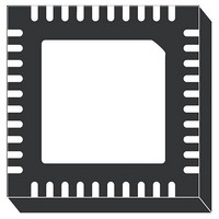
L6756D STMicroelectronics, L6756D Datasheet - Page 32

L6756D
Manufacturer Part Number
L6756D
Description
IC CTLR 2/3/4PH BUCK 40-VFQFPN
Manufacturer
STMicroelectronics
Datasheet
1.L6756DTR.pdf
(36 pages)
Specifications of L6756D
Applications
Controller, Intel VR10, VR11, VR11.1
Voltage - Input
12V
Number Of Outputs
4
Voltage - Output
0.3 ~ 1.6 V
Operating Temperature
0°C ~ 70°C
Mounting Type
Surface Mount
Package / Case
40-VFQFN, 40-VFQFPN
Output Voltage
3 V
Input Voltage
- 0.3 V to + 15 V
Switching Frequency
185 KHz to 215 KHz
Operating Temperature Range
- 40 C to + 150 C
Mounting Style
SMD/SMT
Lead Free Status / RoHS Status
Lead free / RoHS Compliant
Available stocks
Company
Part Number
Manufacturer
Quantity
Price
System control loop compensation
Note:
9.2
32/36
The introduction of a capacitor (C
response by coupling the output voltage dV/dt on the FB pin so using the error amplifier as a
comparator. The COMP pin will suddenly reacts and, also thanks to the LTB Technology
control scheme, all the phases can be turned on together to immediately give to the output
the required energy. Typical design considers to start from values in the range of 100pF
validating the effect by bench testing. Additional series resistor (R
LTB Technology
LTB Technology
by reducing the system latencies and immediately turning ON all the phases to provide the
correct amount of energy to the load. By properly deigning the LTB network as well as the
LTB gain, the undershoot and the ring-back can be minimized also optimizing the output
capacitors count.
LTB Technology
Transients with selected dV/dt, it cancels the interleaved phase-shift, turning-on
simultaneously all phases. it then implements a parallel, independent loop that reacts to
Load-Transients bypassing E/A latencies.
LTB Technology
Figure 16. LTB Technology
The LTB detector is able to detect output load transients by coupling the output voltage
through an R
then compared with the COMP pin level. The resulting duty-cycle programmed is then OR-
ed with the PWMx signal of each phase by-passing the main control loop. All the phases will
then be turned-on together and the EA latencies results bypassed as well.
LTB
®
®
®
- C
further enhances the performances of dual-edge asynchronous systems
monitors the output voltage through a dedicated pin detecting Load-
control loop is reported in
LTB
network. After detecting a load transient, the LTB ramp is reset and
®
®
control loop
I
) in parallel to R
Figure
FB
16.
significantly speeds-up the transient
I
) can also be used.
L6756D
®


